SLLS872J January 2008 – March 2023 SN65HVD1785 , SN65HVD1786 , SN65HVD1787 , SN65HVD1791 , SN65HVD1792 , SN65HVD1793
PRODUCTION DATA
- 1 Features
- 2 Applications
- 3 Description
- 4 Revision History
- 5 Product Selection Guide
- 6 Pin Configuration and Functions
- 7 Specifications
- 8 Parameter Measurement Information
- 9 Detailed Description
- 10Application and Implementation
- 11Power Supply Recommendations
- 12Layout
- 13Device and Documentation Support
- 14Mechanical, Packaging, and Orderable Information
Package Options
Mechanical Data (Package|Pins)
- D|8
Thermal pad, mechanical data (Package|Pins)
- D|8
Orderable Information
3 Description
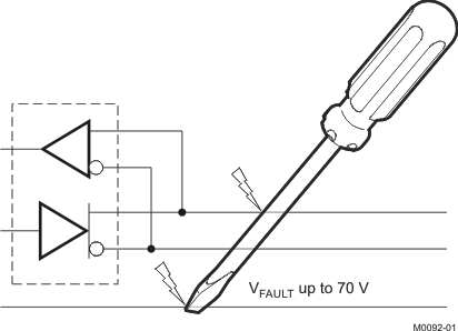
These devices are designed to survive overvoltage faults such as direct shorts to power supplies, mis-wiring faults, connector failures, cable crushes, and tool mis-applications. They are also robust to ESD events, with high levels of protection to human-body model specifications.
These devices combine a differential driver and a differential receiver, which operate from a single power supply. In the 'HVD1785, 'HVD1786, and 'HVD1787, the driver differential outputs and the receiver differential inputs are connected internally to form a bus port suitable for half-duplex (two-wire bus) communication. In the 'HVD1793, the driver differential outputs and the receiver differential inputs are separate pins, to form a bus port suitable for full-duplex (four-wire bus) communication. These ports feature a wide common-mode voltage range, making the devices suitable for multipoint applications over long cable runs. These devices are characterized from –40°C to 105°C.
For similar features with 3.3-V supply operation, see the SN65HVD1781 (SLLS877).
| PART NUMBER | PACKAGE(1) | BODY SIZE (NOM) |
|---|---|---|
| SN65HVD1785, SN65HVD1786, SN65HVD1787 | SOIC (8) | 4.90 mm × 3.91 mm |
| PDIP (8) | 9.81 mm × 6.35 mm | |
| SN65HVD1791, SN65HVD1792, SN65HVD1793 | SOIC (14) | 8.65 mm × 3.91 mm |
 Example of Bus Short to Power Supply