SLLS552G December 2002 – September 2022 SN65HVD20 , SN65HVD21 , SN65HVD22 , SN65HVD23 , SN65HVD24
PRODUCTION DATA
- 1 Features
- 2 Applications
- 3 Description
- 4 Revision History
- 5 Description (continued)
- 6 Device Comparison
- 7 Pin Configuration and Functions
-
8 Specifications
- 8.1 Absolute Maximum Ratings
- 8.2 ESD Ratings
- 8.3 Recommended Operating Conditions
- 8.4 Thermal Information
- 8.5 Driver Electrical Characteristics
- 8.6 Receiver Electrical Characteristics
- 8.7 Driver Switching Characteristics
- 8.8 Receiver Switching Characteristics
- 8.9 Receiver Equalization Characteristics
- 8.10 Power Dissipation
- 8.11 Typical Characteristics
- 9 Parameter Measurement Information
- 10Detailed Description
- 11Application and Implementation
- 12Power Supply Recommendations
- 13Layout
- 14Device and Documentation Support
- 15Mechanical, Packaging, and Orderable Information
Package Options
Mechanical Data (Package|Pins)
Thermal pad, mechanical data (Package|Pins)
Orderable Information
11.2.3 Application Curves
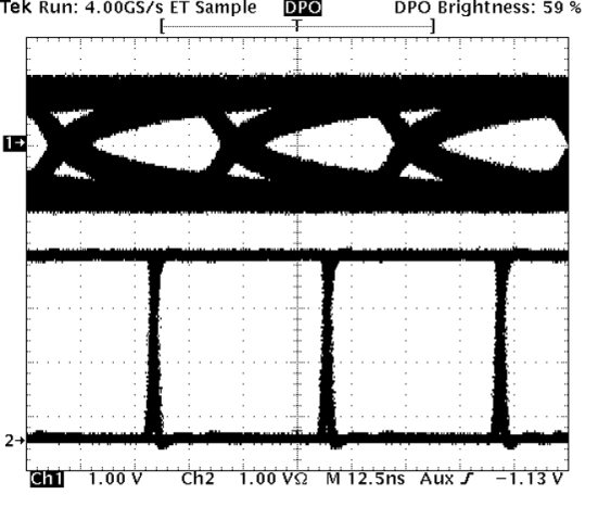
Figure 11-2 illustrates the benefits of integrated receiver equalization as implemented in the SN65HVD23 transceiver. In this test setup, a differential signal generator applied a signal voltage at one end of the cable, which was Belden 3105A twisted-pair shielded cable. The test signal was a pseudo-random bit stream (PRBS) of nonreturn-to-zero (NRZ) data. Channel 1 (top) shows the eye-pattern of the differential voltage at the receiver inputs (after the cable attenuation). Channel 2 (bottom) shows the output of the receiver.
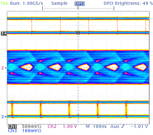
Figure 11-3 illustrates the benefits of integrated receiver equalization as implemented in the SN65HVD24 transceiver. In this test setup, a differential signal generator applied a signal voltage at one end of the cable, which was Belden 3105A twisted-pair shielded cable. The test signal was a pseudo-random bit stream (PRBS) of nonreturn-to-zero (NRZ) data. Channel 1 (top) shows the eye-pattern of the bit stream. Channel 2 (middle) shows the eye-pattern of the differential voltage at the receiver inputs (after the cable attenuation). Channel 3 (bottom) shows the output of the receiver.
 Figure 11-2 SN65HVD23 Receiver Performance at 25 Mbps Over 150 Meter Cable
 Figure 11-3 SN65HVD24 Receiver Performance at 5 Mbps Over 500 Meter Cable