SLLS552G December 2002 – September 2022 SN65HVD20 , SN65HVD21 , SN65HVD22 , SN65HVD23 , SN65HVD24
PRODUCTION DATA
- 1 Features
- 2 Applications
- 3 Description
- 4 Revision History
- 5 Description (continued)
- 6 Device Comparison
- 7 Pin Configuration and Functions
-
8 Specifications
- 8.1 Absolute Maximum Ratings
- 8.2 ESD Ratings
- 8.3 Recommended Operating Conditions
- 8.4 Thermal Information
- 8.5 Driver Electrical Characteristics
- 8.6 Receiver Electrical Characteristics
- 8.7 Driver Switching Characteristics
- 8.8 Receiver Switching Characteristics
- 8.9 Receiver Equalization Characteristics
- 8.10 Power Dissipation
- 8.11 Typical Characteristics
- 9 Parameter Measurement Information
- 10Detailed Description
- 11Application and Implementation
- 12Power Supply Recommendations
- 13Layout
- 14Device and Documentation Support
- 15Mechanical, Packaging, and Orderable Information
Package Options
Mechanical Data (Package|Pins)
Thermal pad, mechanical data (Package|Pins)
Orderable Information
10.3 Feature Description
The SN65HVD2x family of devices integrates a differential receiver and differential driver with additional features for improved performance in electrically-noisy, long-cable, or other fault-intolerant applications.
The receiver hysteresis (typically 130 mV) is much larger than found in typical RS-485 transceivers. This helps reject spurious noise signals which would otherwise cause false changes in the receiver output state.
Slew rate limiting on the driver outputs (SN65HVD2[1,2,4]) reduces the high-frequency content of signal edges. This decreases reflections from bus discontinuities, and allows longer stub lengths between nodes and the main bus line. Designers must consider the maximum signaling rate and cable length required for a specific application, and choose the transceiver best matching those requirements.
When DE is low, the differential driver is disabled, and the A and B outputs are in high-impedance states. When DE is high, the differential driver is enabled, and drives the A and B outputs according to the state of the D inputs.
When RE is high, the differential receiver output buffer is disabled, and the R output is in a high-impedance state. When RE is low, the differential receiver is enabled, and the R output reflects the state of the differential bus inputs on the A and B pins.
If both the driver and receiver are disabled, (DE low and RE high) then all nonessential circuitry, including auxiliary functions such as failsafe and receiver equalization is placed in a low-power standby state. This reduces power consumption to less than 5 µW. When either enable input is asserted, the circuitry again becomes active.
In addition to the primary differential receiver, these devices incorporate a set of comparators and logic to implement an active receiver failsafe feature. These components determine whether the differential bus signal is valid. Whenever the differential signal is close to zero volts (neither high nor low), a timer initiates, If the differential input remains within the transition range for more than 250 µs, the timer expires and set the receiver output to the high state. If a valid bus input (high or low) is received at any time, the receiver output reflects the valid bus state, and the timer is reset.
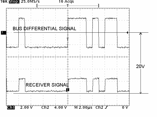
 Figure 10-1 SN65HVD22 Receiver Operation With 20-V Offset on Input Signal
 Figure 10-2 Cable Attenuation Model for Jitter Measurements