SLLSES4A September 2016 – November 2016 SN65HVD233-Q1 , SN65HVD234-Q1 , SN65HVD235-Q1
PRODUCTION DATA.
- 1 Features
- 2 Applications
- 3 Description
- 4 Revision History
- 5 Description (continued)
- 6 Device Comparison Table
- 7 Pin Configuration and Functions
-
8 Specifications
- 8.1 Absolute Maximum Ratings
- 8.2 ESD Ratings
- 8.3 Recommended Operating Conditions
- 8.4 Thermal Information
- 8.5 Electrical Characteristics: Driver
- 8.6 Electrical Characteristics: Receiver
- 8.7 Switching Characteristics: Driver
- 8.8 Switching Characteristics: Receiver
- 8.9 Switching Characteristics: Device
- 8.10 Typical Characteristics
- 9 Parameter Measurement Information
- 10Detailed Description
- 11Application and Implementation
- 12Power Supply Recommendations
- 13Layout
- 14Device and Documentation Support
- 15Mechanical, Packaging, and Orderable Information
Package Options
Mechanical Data (Package|Pins)
- D|8
Thermal pad, mechanical data (Package|Pins)
Orderable Information
1 Features
- Compatible With ISO 11898-2
- Qualified for Automotive Applications
- AEC-Q100 Qualified With the Following Results:
- Device Temperature Grade 1: –40°C to 125°C Ambient Operating Temperature Range
- Device HBM ESD Classification Levels
- Bus Pins: ±12 000 V
- Other Pins: ±3 000 V
- Device CDM ESD Classification Level ±1 000 V
- Single 3.3-V Supply Voltage
- Bit Rates up to 1 Mbps
- Bus Pins Fault Protection up to ±36 V
- –7-V to 12-V Common-Mode Range
- High Input Impedance Allows for 120 Nodes
- LVTTL I/Os are 5-V Tolerant
- GIFT/ICT Compliant
- Adjustable Driver Slew Rates for Improved Emissions Performance
- Unpowered Node Does Not Disturb the Bus
- Low-Current Standby Mode, 200-μA (Typical)
- Average Power Dissipation: 36.4 mW
- SN65HVD233-Q1: Loopback Mode
- SN65HVD234-Q1: Ultralow-Current Sleep Mode
- 50-nA Typical Current Consumption
- SN65HVD235-Q1: Autobaud Loopback Mode
- Thermal Shutdown Protection
- Power Up and Down With Glitch-Free Bus Inputs and Outputs
- High Input Impedance With Low VCC
- Monotonic Output During Power Cycling
2 Applications
- In-Vehicle Networking
- Advanced Driver-Assistance Systems (ADAS)
- Body Electronics and Lighting
- Infotainment and Cluster
- Hybrid, Electric, and Powertrain Systems
- Applications in Accordance With CAN Bus Standards Such as NMEA 2000 and SAE J1939
3 Description
The SN65HVD233-Q1, SN65HVD234-Q1, and SN65HVD235-Q1 devices are fault-protected 3.3-V CAN transceivers that are qualified for use in automotive applications. These transceivers work from a 3.3-V supply and are ideal for systems that also leverage a 3.3-V microcontroller, thereby reducing the need for additional components or a separate supply to power the controller and the CAN transceiver. The SN65HVD23x-Q1 transceivers are compatible with the ISO 11898-2 standard and thus are interoperable in mixed networks that employ 5-V CAN and/or 3.3-V CAN transceivers.
Designed for operation in especially harsh environments, the devices feature crosswire protection, overvoltage protection on the CANH and CANL pins up to ±36 V, loss-of-ground protection, overtemperature (thermal shutdown) protection, and common-mode transient protection of ±100 V. These devices operate over a wide –7-V to 12-V common-mode range. These transceivers are the interface between the host CAN controller on the microprocessor and the differential CAN bus used in transportation and automotive applications.
Device Information(1)
| PART NUMBER | PACKAGE | BODY SIZE (NOM) |
|---|---|---|
| SN65HVD233-Q1 | SOIC (8) | 4.90 mm × 3.91 mm |
| SN65HVD234-Q1 | ||
| SN65HVD235-Q1 |
- For all available packages, see the orderable addendum at the end of the data sheet.
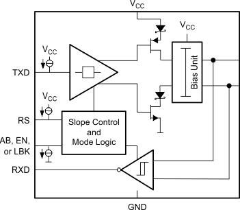
Block Diagram
