SLLS557H November 2002 – November 2018 SN65HVD233 , SN65HVD234 , SN65HVD235
PRODUCTION DATA.
- 1 Features
- 2 Applications
- 3 Description
- 4 Revision History
- 5 Description (continued)
- 6 Device Comparison Table
- 7 Pin Configuration and Functions
-
8 Specifications
- 8.1 Absolute Maximum Ratings
- 8.2 ESD Ratings
- 8.3 Recommended Operating Conditions
- 8.4 Thermal Information
- 8.5 Power Dissipation Ratings
- 8.6 Electrical Characteristics: Driver
- 8.7 Electrical Characteristics: Receiver
- 8.8 Switching Characteristics: Driver
- 8.9 Switching Characteristics: Receiver
- 8.10 Switching Characteristics: Device
- 8.11 Typical Characteristics
- 9 Parameter Measurement Information
- 10Detailed Description
- 11Application and Implementation
- 12Power Supply Recommendations
- 13Layout
- 14Device and Documentation Support
- 15Mechanical, Packaging, and Orderable Information
Package Options
Refer to the PDF data sheet for device specific package drawings
Mechanical Data (Package|Pins)
- D|8
Thermal pad, mechanical data (Package|Pins)
Orderable Information
11.2.3 Application Curve
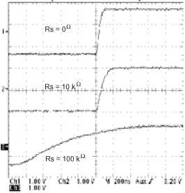
Figure 39 shows 3 typical output waveforms for the SN65HVD233 device with three different connections made to the RS pin. The top waveform show the typical differential signal when transitioning from a recessive level to a dominant level on the CAN bus with RS tied to GND through a 0-Ω resistor. The second waveform shows the same signal for the condition with a 10-kΩ resistor tied from RS to ground. The bottom waveform shows the typical differential signal for the case where a 100-kΩ resistor is tied from the RS pin to ground.
 Figure 39. Typical SN65HVD233 Output Waveforms With Different Slope Control Resistor Values