SLLSEI3A September 2013 – November 2015 SN65HVD265 , SN65HVD266 , SN65HVD267
PRODUCTION DATA.
- 1 Features
- 2 Applications
- 3 Description
- 4 Revision History
- 5 Device Comparison Table
- 6 Pin Configurations and Functions
- 7 Specifications
- 8 Parameter Measurement Information
- 9 Detailed Description
- 10Application and Implementation
- 11Power Supply Recommendations
- 12Layout
- 13Device and Documentation Support
- 14Mechanical, Packaging, and Orderable Information
Package Options
Mechanical Data (Package|Pins)
- D|8
Thermal pad, mechanical data (Package|Pins)
Orderable Information
8 Parameter Measurement Information
 Figure 2. RXD Dominant Timeout Test Circuit and Measurement
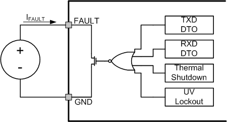 Figure 3. FAULT Test and Measurement
 Figure 4. Driver Test Circuit and Measurement
 Figure 5. Receiver Test Circuit and Measurement
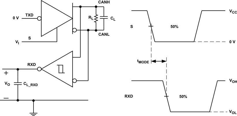 Figure 6. tMODE Test Circuit and Measurement
Table 1. Receiver Differential Input Voltage Threshold Test
| INPUT | OUTPUT | |||
|---|---|---|---|---|
| VCANH | VCANL | |VID| | RXD | |
| -1.1V | -2.0 V | 900 mV | L | VOL |
| 7.0 V | 6.1 V | 900 mV | L | |
| -1.5 V | -2.0 V | 500 mV | H | VOH |
| 7.0 V | 6.5 V | 500 mV | H | |
| Open | Open | X | H | |
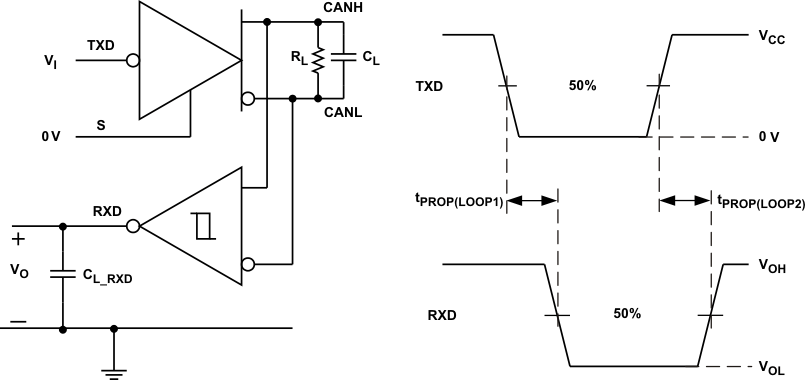 Figure 7. TPROP(LOOP) Test Circuit and Measurement
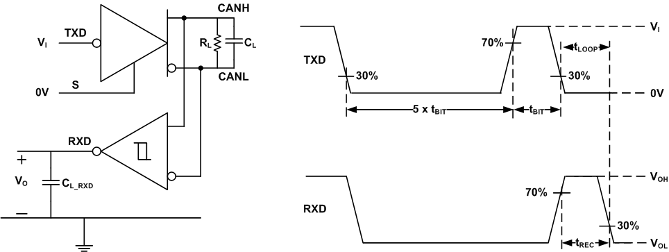
Note: tLOOP is equivalent to tPROP(LOOP) from CAN timing.
Figure 8. Loop Delay Symmetry Test Circuit and Measurement
 Figure 9. TXD Dominant Timeout Test Circuit and Measurement
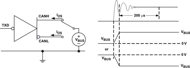 Figure 10. Driver Short Circuit Current Test and Measurement