SLLS162F July 1993 – April 2024 SN65LBC174 , SN75LBC174
PRODUCTION DATA
- 1
- 1 Features
- 2 Applications
- 3 Description
- 4 Pin Configuration and Functions
- 5 Specifications
- 6 Parameter Measurement Information
- 7 Detailed Description
- 8 Device and Documentation Support
- 9 Revision History
- 10Mechanical, Packaging, and Orderable Information
Package Options
Refer to the PDF data sheet for device specific package drawings
Mechanical Data (Package|Pins)
- N|16
- DW|20
Thermal pad, mechanical data (Package|Pins)
Orderable Information
4 Pin Configuration and Functions
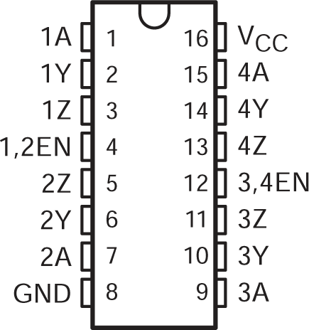
 Figure 4-1 N Package (Top View)
Table 4-1 Pin Functions
| PIN | TYPE(1) | DESCRIPTION | |
|---|---|---|---|
| NAME | NO. | ||
| 1A | 1 | I | Driver 1 input |
| 1Y | 2 | O | Driver 1 output |
| 1Z | 3 | O | Driver 1 inverted output |
| 1,2EN | 4 | I | Active high driver enable channel 1 and 2 |
| 2Z | 5 | O | Driver 2 inverted output |
| 2Y | 6 | O | Driver 2 output |
| 2A | 7 | I | Driver 2 input |
| GND | 8 | - | Ground pin |
| 3A | 9 | I | Driver 3 input |
| 3Y | 10 | O | Driver 3 output |
| 3Z | 11 | O | Driver 3 inverted output |
| 3,4EN | 12 | I | Active high driver enable channel 3 and 4 |
| 4Z | 13 | O | Driver 4 inverted output |
| 4Y | 14 | O | Driver 4 output |
| 4A | 15 | I | Driver 4 input |
| VCC | 16 | ̶ | Power pin |
(1) Signal Types: I = Input, O = Output, I/O = Input or Output.
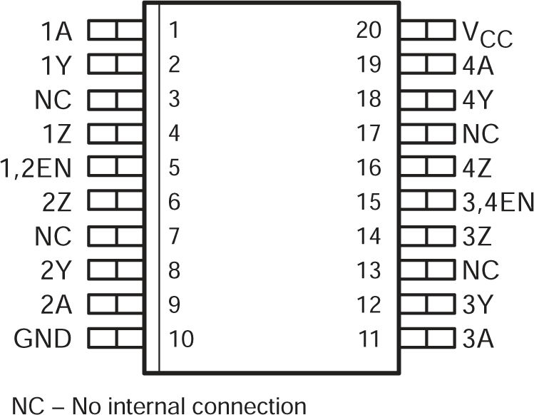
 Figure 4-2 DW Package (Top View)
Table 4-2 Pin Functions
| PIN | TYPE(1) | DESCRIPTION | |
|---|---|---|---|
| NAME | NO. | ||
| 1A | 1 | I | Driver 1 input |
| 1Y | 2 | O | Driver 1 output |
| NC | 3 | - | No Internal Connection |
| 1Z | 4 | O | Driver 1 inverted output |
| 1,2EN | 5 | I | Active high driver enable channel 1 and 2 |
| 2Z | 6 | O | Driver2 inverted output |
| NC | 7 | - | No Internal Connection |
| 2Y | 8 | O | Driver 2 output |
| 2A | 9 | I | Driver 2 input |
| GND | 10 | ̶ | Ground pin |
| 3A | 11 | I | Driver 3 input |
| 3Y | 12 | O | Driver 3 output |
| NC | 13 | ̶ | No Internal Connection |
| 3Z | 14 | O | Driver 3 inverted output |
| 3,4EN | 15 | I | Active high driver enable channel 3 and 4 |
| 4Z | 16 | O | Driver 4 inverted output |
| NC | 17 | ̶ | No Internal Connection |
| 4Y | 18 | O | Driver 4 output |
| 4A | 19 | I | Driver 4 input |
| VCC | 20 | ̶ | Power pin |
(1) Signal Types: I = Input, O = Output, I/O = Input or Output.