SLLS236I October 1996 – June 2015 SN65LBC184 , SN75LBC184
PRODUCTION DATA.
- 1 Features
- 2 Applications
- 3 Description
- 4 Revision History
- 5 Pin Configuration and Functions
-
6 Specifications
- 6.1 Absolute Maximum Ratings
- 6.2 ESD Ratings
- 6.3 Recommended Operating Conditions
- 6.4 Thermal Information
- 6.5 Electrical Characteristics: Driver
- 6.6 Electrical Characteristics: Receiver
- 6.7 Driver Switching Characteristics
- 6.8 Receiver Switching Characteristics
- 6.9 Dissipation Ratings
- 6.10 Typical Characteristics
- 7 Parameter Measurement Information
- 8 Detailed Description
- 9 Application and Implementation
- 10Power Supply Recommendations
- 11Layout
- 12Device and Documentation Support
- 13Mechanical, Packaging, and Orderable Information
Package Options
Mechanical Data (Package|Pins)
Thermal pad, mechanical data (Package|Pins)
Orderable Information
7 Parameter Measurement Information

A. The input pulse is supplied by a generator having the following characteristics: PRR = 1.25 kHz, 50% duty cycle, tr ≤ 10 ns, tf ≤ 10 ns, ZO = 50 Ω.
B. CL includes probe and jig capacitance.
Figure 6. Driver tPZH and tPHZ Test Circuit and Voltage Waveforms

A. The input pulse is supplied by a generator having the following characteristics: PRR = 1.25 kHz, 50% duty cycle, tr ≤ 10 ns, tf ≤ 10 ns, ZO = 50 Ω.
B. CL includes probe and jig capacitance.
Figure 7. Driver tPZL and tPLZ Test Circuit and Voltage Waveforms
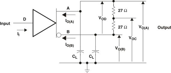
A. Resistance values are in ohms and are 1% tolerance.
B. CL includes probe and jig capacitance.
Figure 8. Driver Test Circuit, Voltage, and Current Definitions
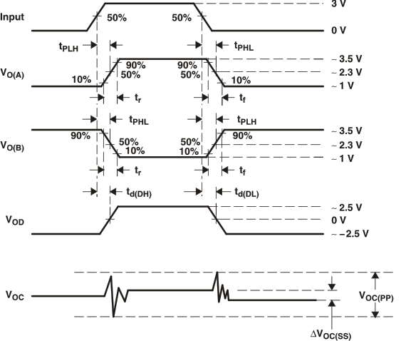 Figure 9. Driver Timing, Voltage, and Current Waveforms
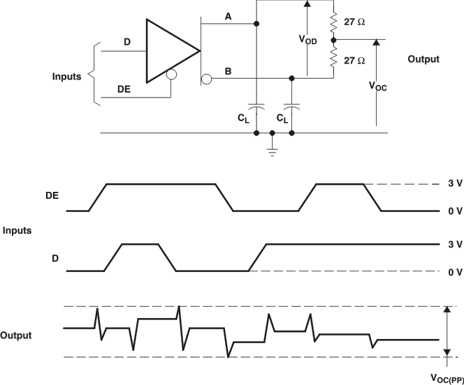
A. Resistance values are in ohms and are 1% tolerance.
B. CL includes probe and jig capacitance (±10%).
Figure 10. Driver VOC(PP) Test Circuit and Waveforms
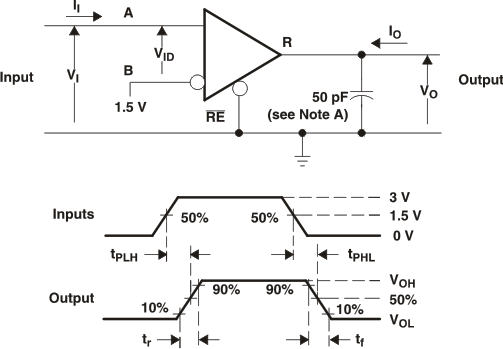
A. This value includes probe and jig capacitance (±10%).
Figure 11. Receiver tPLH and tPHL Test Circuit and Voltage Waveforms
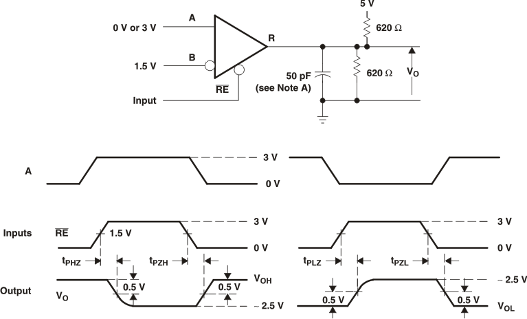
A. This value includes probe and jig capacitance (±10%).
Figure 12. Receiver tPZL, tPLZ, tPZH, and tPHZ Test Circuit and Voltage Waveforms