SLLSEH7B December 2013 – June 2016 SN65LVPE512
PRODUCTION DATA.
- 1 Features
- 2 Applications
- 3 Description
- 4 Revision History
- 5 Pin Configuration and Functions
- 6 Specifications
- 7 Parameter Measurement Information
- 8 Detailed Description
- 9 Application and Implementation
- 10Power Supply Recommendations
- 11Layout
- 12Device and Documentation Support
- 13Mechanical, Packaging, and Orderable Information
Package Options
Mechanical Data (Package|Pins)
Thermal pad, mechanical data (Package|Pins)
- RGE|24
Orderable Information
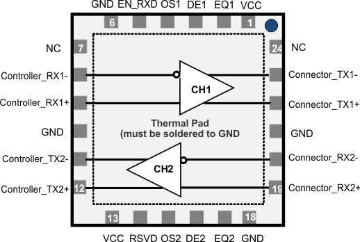
5 Pin Configuration and Functions
RGE Package
24-Pin VQFN
Top View

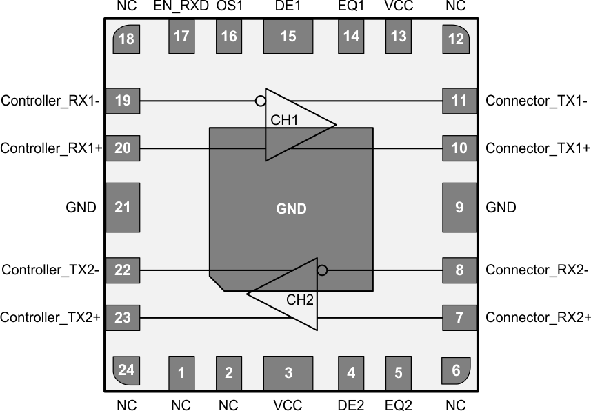
RMQ Package
24-Pin WQFN
Top View

Pin Functions
| PIN | I/O TYPE | DESCRIPTION | |||
|---|---|---|---|---|---|
| NAME | VQFN | WQFN | |||
| HIGH SPEED DIFFERENTIAL I/O PINS | |||||
| Controller_RX1– | 8 | 19 | I, CML | Non-inverting and inverting CML differential input for CH1 and CH2. These pins are tied to an internal voltage bias by dual termination resistor circuit. Pins labeled Controller must connect to the USB 3.0 host or device controller. Pins labeled Connector must connect to the USB 3.0 connector. |
|
| Controller_RX1+ | 9 | 20 | I, CML | ||
| Connector_RX2– | 20 | 8 | I, CML | ||
| Connector_RX2+ | 19 | 7 | I, CML | ||
| Connector_TX1– | 23 | 11 | O, CML | Non-inverting and inverting CML differential output for CH1 and CH2. These pins are tied to an internal voltage bias by termination resistors. Pins labeled Controller must connect to the USB 3.0 host or device controller. Pins labeled Connector must connect to the USB 3.0 connector. |
|
| Connector_TX1+ | 22 | 10 | O, CML | ||
| Controller_TX2– | 11 | 22 | O, CML | ||
| Controller_TX2+ | 12 | 23 | O, CML | ||
| DEVICE CONTROL PIN | |||||
| EN_RXD | 5 | 17 | I, LVCMOS | Sets device operation modes per Table 4. Internally pulled to VCC. | |
| RSVD | 14 | — | I, LVCMOS | RSVD. Can be left as No-Connect. | |
| NC | 7, 24 | 1, 2, 6, 12, 18, 24 | No-Connect | Pads are not internally connected. | |
| EQ CONTROL PINS(1) | |||||
| DE1, DE2 | 3, 16 | 15, 4 | I, LVCMOS | Selects de-emphasis settings for CH1 and CH2 per Table 4. Internally tied to VCC/2 | |
| EQ1, EQ2 | 2, 17 | 14, 5 | I, LVCMOS | Selects equalization settings for CH1 and CH2 per Table 4. Internally tied to VCC/2 | |
| OS1, OS2 | 4, 15 | 16, NC (2) | I, LVCMOS | Selects output amplitude for CH1 and CH2 per Table 4. Internally tied to VCC/2 | |
| POWER PINS | |||||
| VCC | 1,13 | 3 | Power | Positive supply; must be 3.3 V ±10% | |
| GND | 6, 10, 18, 21, Thermal Pad | 9, Thermal Pad | Power | Supply Ground | |
(1) Internally biased to VCC/2 with > 200-kΩ pullup or pulldown. When pins are left as NC board leakage at this pin pad must be < 1 µA otherwise drive to VCC/2 to assert mid-level state
(2) The RMQ has OS2 internally No-Connect, to select the 1042 mVpp level on TX2.