SCAS974 March 2024 SN74ACT8541
PRODUCTION DATA
- 1
- 1 Features
- 2 Applications
- 3 Description
- 4 Pin Configuration and Functions
- 5 Specifications
- 6 Detailed Description
- 7 Application and Implementation
- 8 Device and Documentation Support
- 9 Revision History
- 10Mechanical, Packaging, and Orderable Information
Package Options
Refer to the PDF data sheet for device specific package drawings
Mechanical Data (Package|Pins)
- RKS|20
- DGS|20
- PW|20
Thermal pad, mechanical data (Package|Pins)
- RKS|20
Orderable Information
3 Description
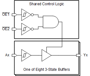
The SN74ACT8541 contains eight independent buffers with 3-state outputs and Schmitt-trigger inputs. All channels can be simultaneously forced into the high-impedance state using either of the output enable inputs (OE1 or OE2).
Package
Information
| PART NUMBER | PACKAGE(1) | PACKAGE SIZE(3) | BODY SIZE (NOM)(3) |
|---|---|---|---|
| SN74ACT8541 | RKS (VQFN, 20) | 4.5mm × 2.5mm | 4.5mm × 2.5mm |
| PW (TSSOP, 20) | 6.5mm × 6.4mm | 6.5mm × 4.4mm | |
| DGS (VSSOP, 20) | 5.1mm × 4.9mm | 5.1mm × 3mm |
(1) For more information, see Section 10.
(3) The package size (length × width) is a nominal value and includes pins, where
applicable
(3) The body size (length × width) is a nominal value and does not include
pins.
 Logic
Diagram (Positive Logic)