SCLS242L October 1995 – September 2014 SN54AHC573 , SN74AHC573
PRODUCTION DATA.
- 1 Features
- 2 Applications
- 3 Description
- 4 Simplified Schematic
- 5 Revision History
- 6 Pin Configuration and Functions
-
7 Specifications
- 7.1 Absolute Maximum Ratings
- 7.2 Handling Ratings
- 7.3 Recommended Operating Conditions
- 7.4 Thermal Information
- 7.5 Electrical Characteristics
- 7.6 Timing Requirements, VCC = 3.3 V ± 0.3 V
- 7.7 Timing Requirements, VCC = 5 V ± 0.5 V
- 7.8 Switching Characteristics, VCC = 3.3 V ± 0.3 V
- 7.9 Switching Characteristics, VCC = 5 V ± 0.5 V
- 7.10 Noise Characteristics
- 7.11 Operating Characteristics
- 7.12 Typical Characteristics
- 8 Parameter Measurement Information
- 9 Detailed Description
- 10Application and Implementation
- 11Power Supply Recommendations
- 12Layout
- 13Device and Documentation Support
- 14Mechanical, Packaging, and Orderable Information
Package Options
Refer to the PDF data sheet for device specific package drawings
Mechanical Data (Package|Pins)
- DGV|20
- DB|20
- NS|20
- N|20
- DW|20
- PW|20
Thermal pad, mechanical data (Package|Pins)
- PW|20
Orderable Information
9 Detailed Description
9.1 Overview
The SNx4AHC573 devices are octal transparent D-type latches designed for 2-V to 5.5-V VCC operation.
When the latch-enable (LE) input is high, the Q outputs follow the data (D) inputs. When LE is low, the Q outputs are latched at the logic levels of the D inputs.
A buffered output-enable (OE) input can be used to place the eight outputs in either a normal logic state (high or low) or the high-impedance state. In the high-impedance state, the outputs neither load nor drive the bus lines significantly. The high-impedance state and increased drive provide the capability to drive bus lines without interface or pull-up components.
OE does not affect the internal operations of the latches. Old data can be retained or new data can be entered while the outputs are in the high-impedance state.
To ensure the high-impedance state during power up or power down, OE should be tied to VCC through a pull-up resistor; the minimum value of the resistor is determined by the current-sinking capability of the driver.
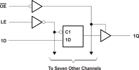
9.2 Functional Block Diagram
9.3 Feature Description
- Wide operating voltage range
- Operates from 2 V to 5.5 V
- Allows down voltage translation
- Inputs accept voltages to 5.5 V
- Slow edges reduce output ringing
9.4 Device Functional Modes
Table 1. Function Table
(Each Latch)
| INPUTS | OUTPUT Q |
||
|---|---|---|---|
| OE | LE | D | |
| L | H | H | H |
| L | H | L | L |
| L | L | X | Q0 |
| H | X | X | Z |