SCLS418H June 1998 – December 2014 SN74AHCT367
PRODUCTION DATA.
- 1 Features
- 2 Applications
- 3 Description
- 4 Simplified Schematic
- 5 Revision History
- 6 Pin Configuration and Functions
- 7 Specifications
- 8 Parameter Measurement Information
- 9 Detailed Description
- 10Application and Implementation
- 11Power Supply Recommendations
- 12Layout
- 13Mechanical, Packaging, and Orderable Information
Package Options
Refer to the PDF data sheet for device specific package drawings
Mechanical Data (Package|Pins)
- DB|16
- PW|16
- D|16
- DGV|16
Thermal pad, mechanical data (Package|Pins)
- D|16
Orderable Information
9 Detailed Description
9.1 Overview
The SN74AHCT367 device is designed specifically to improve both the performance and density of
3-state memory address drivers, clock drivers, and bus-oriented receivers and transmitters. This device is organized as a dual 4-line and 2-line buffer/driver with active-low output-enable (1OE and 2OE) inputs. When OE is low, the device passes noninverted data from the A inputs to the Y outputs. When OE is high, the outputs are in the high-impedance state.
To ensure the high-impedance state during power up or power down, OE should be tied to VCC through a pull-up resistor; the minimum value of the resistor is determined by the current-sinking capability of the driver.
9.2 Functional Block Diagram
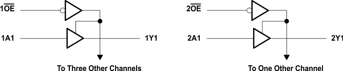 Figure 3. Logic Diagram (Positive Logic)
9.3 Feature Description
- VCC is optimized at 5 V
- Allows up voltage translation from 3.3 V to 5 V
- Inputs Accept VIH levels of 2 V
- Slow edge rates minimize output ringing
- Inputs are TTL-Voltage compatible
9.4 Device Functional Modes
Table 1. Function Table
(Each Buffer/Driver)
| INPUTS | OUTPUT Y |
|
|---|---|---|
| OE | A | |
| H | X | Z |
| L | H | H |
| L | L | L |