SCES503J NOVEMBER 2003 – June 2015 SN74AUP1G57
PRODUCTION DATA.
- 1 Features
- 2 Applications
- 3 Description
- 4 Revision History
- 5 Pin Configuration and Functions
-
6 Specifications
- 6.1 Absolute Maximum Ratings
- 6.2 ESD Ratings
- 6.3 Recommended Operating Conditions
- 6.4 Thermal Information
- 6.5 Electrical Characteristics
- 6.6 Switching Characteristics, CL = 5 pF
- 6.7 Switching Characteristics, CL = 10 pF
- 6.8 Switching Characteristics, CL = 15 pF
- 6.9 Switching Characteristics, CL = 30 pF
- 6.10 Operating Characteristics
- 6.11 Typical Characteristics
- 7 Parameter Measurement Information
- 8 Detailed Description
- 9 Application and Implementation
- 10Power Supply Recommendations
- 11Layout
- 12Device and Documentation Support
- 13Mechanical, Packaging, and Orderable Information
Package Options
Mechanical Data (Package|Pins)
Thermal pad, mechanical data (Package|Pins)
- DRY|6
Orderable Information
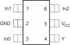
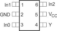
5 Pin Configuration and Functions
DBV Package
6-Pin SOT-23
Top View

DCK Package
6-Pin SC70
Top View

DRL Package
6-Pin SOT
Top View

DRY Package
6-Pin SON
Top View

DSF Package
6-Pin SON
Top View

YFP Package
6-Pin DSBGA
Top View

YZP Package
6-Pin DSBGA
Top View

Pin Functions
| PIN | I/O | DESCRIPTION | ||
|---|---|---|---|---|
| NAME | SOT-23, SC70, SOT | DSBGA | ||
| ln1 | 1 | A1 | I | Logic input 1 |
| GND | 2 | B1 | — | Ground |
| ln0 | 3 | C1 | I | Logic input 0 |
| Y | 4 | C2 | O | Logic output |
| VCC | 5 | B2 | — | Power |
| ln2 | 6 | A2 | I | Logic input 2 |