SCES852A December 2013 – April 2016 SN74AUP1T34-Q1
PRODUCTION DATA.
- 1 Features
- 2 Applications
- 3 Description
- 4 Revision History
- 5 Pin Configuration and Functions
- 6 Specifications
- 7 Parameter Measurement Information
- 8 Detailed Description
- 9 Application and Implementation
- 10Power Supply Recommendations
- 11Layout
- 12Device and Documentation Support
- 13Mechanical, Packaging, and Orderable Information
Package Options
Mechanical Data (Package|Pins)
- DCK|5
Thermal pad, mechanical data (Package|Pins)
Orderable Information
11 Layout
11.1 Layout Guidelines
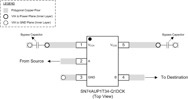
To ensure reliability of the device, TI recommends following common printed-circuit board layout guidelines.
- Bypass capacitors must be used on power supplies.
- Short trace lengths must be used to avoid excessive loading.
- Placing pads on the signal paths for loading capacitors or pullup resistors helps adjust rise and fall times of signals depending on the system requirements.
11.2 Layout Example
 Figure 6. Example Layout