SCDS175A September 2004 – December 2022 SN74CBT3383C
PRODUCTION DATA
- 1 Features
- 2 Applications
- 3 Description
- 4 Revision History
- 5 Description (continued)
- 6 Pin Configuration and Functions
- 7 Specifications
- 8 Parameter Measurement Information
- 9 Detailed Description
- 10Application and Implementation
- 11Power Supply Recommendations
- 12Layout
- 13Device and Documentation Support
- 14Mechanical, Packaging, and Orderable Information
Package Options
Mechanical Data (Package|Pins)
Thermal pad, mechanical data (Package|Pins)
Orderable Information
3 Description
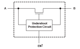
The SN74CBT3383C is a high-speed TTL-compatible FET bus-exchange switch with low ON-state resistance (ron), allowing for minimal propagation delay. Active Undershoot-Protection Circuitry on the A and B ports of the SN74CBT3383C provides protection for undershoot up to −2 V by sensing an undershoot event and ensuring that the switch remains in the proper OFF state.
The SN74CBT3383C is organized as a 10-bit bus switch, or as a 5-bit bus-exchange switch with a single output-enable (BE) input that provides data exchanging between four signal ports. The select (BX) input controls the data path of the bus-exchange switch. When BE is low, the A port is connected to the B port, allowing bidirectional data flow between ports. When BE is high, a high-impedance state exists between the A and B ports.
| PART NUMBER | PACKAGE(1) | BODY SIZE (NOM) |
|---|---|---|
| SN74CBT3383C | DBQ (SSOP, 24) | 8.65 mm × 3.90 mm |
| DW (SOIC, 24) | 15.40 mm × 7.50 mm | |
| PW (TSSOP, 24) | 7.80 mm × 4.40 mm |
 Simplified Schematic, Each FET Switch (SW)