SCLS110F December 1982 – February 2022 SN54HC151 , SN74HC151
PRODUCTION DATA
- 1 Features
- 2 Description
- 3 Revision History
- 4 Pin Configuration and Functions
- 5 Specifications
- 6 Parameter Measurement Information
- 7 Detailed Description
- 8 Power Supply Recommendations
- 9 Layout
- 10Device and Documentation Support
- 11Mechanical, Packaging, and Orderable Information
Package Options
Refer to the PDF data sheet for device specific package drawings
Mechanical Data (Package|Pins)
- PW|16
- |
- NS|16
- N|16
- D|16
Thermal pad, mechanical data (Package|Pins)
Orderable Information
2 Description
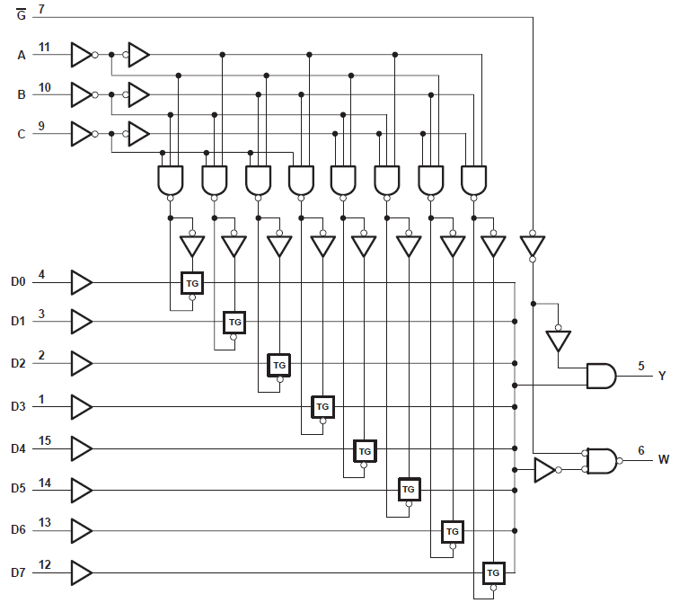
This data selector/multiplexer provides full binary decoding to select one of eight data sources. The strobe (G) input must be at a low logic level to enable the inputs. A high level at the strobe terminal forces the standard output (Y) low and the inverted output (W) high.
Device Information
| PART NUMBER | PACKAGE(1) | BODY SIZE (NOM) |
|---|---|---|
| SN54HC151J | CDIP (16) | 24.38 mm × 6.92 mm |
| SN74HC151D | SOIC (16) | 9.90 mm × 3.90 mm |
| SN74HC151N | PDIP (16) | 19.31 mm × 6.35 mm |
| SN74HC151NS | SO (16) | 6.20 mm × 5.30 mm |
| SN74HC151PW | TSSOP (16) | 5.00 mm × 4.40 mm |
| SNJ54HC151FK | LCCC (20) | 8.89 mm × 8.45 mm |
(1) For all available packages, see the
orderable addendum at the end of the data sheet.

Pin numbers shown are for the D, J, N, NS, PW, and W packages.
Functional Block Diagram