SCES337K May 2000 – October 2014 SN74LV07A
PRODUCTION DATA.
- 1 Features
- 2 Applications
- 3 Description
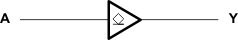
- 4 Simplified Schematic
- 5 Revision History
- 6 Pin Configuration and Functions
-
7 Specifications
- 7.1 Absolute Maximum Ratings
- 7.2 Handling Ratings
- 7.3 Recommended Operating Conditions
- 7.4 Thermal Information
- 7.5 Electrical Characteristics
- 7.6 Switching Characteristics, VCC = 2.5 V ± 0.2 V
- 7.7 Switching Characteristics, VCC = 3.3 V ± 0.3 V
- 7.8 Switching Characteristics, VCC = 5 V ± 0.5 V
- 7.9 Noise Characteristics
- 7.10 Operating Characteristics
- 7.11 Typical Characteristics
- 8 Parameter Measurement Information
- 9 Detailed Description
- 10Application and Implementation
- 11Power Supply Recommendations
- 12Layout
- 13Device and Documentation Support
- 14Mechanical, Packaging, and Orderable Information
Package Options
Refer to the PDF data sheet for device specific package drawings
Mechanical Data (Package|Pins)
- D|14
- DB|14
- DGV|14
- PW|14
- NS|14
Thermal pad, mechanical data (Package|Pins)
Orderable Information
1 Features
- 2-V to 5.5-V VCC Operation
- Typical VOLP (Output Ground Bounce)
< 0.8 V at VCC = 3.3 V, TA = 25°C - Typical VOHV (Output VOH Undershoot)
> 2.3 V at VCC = 3.3 V, TA = 25°C - Outputs are Disabled During Power Up
and Power Down With Inputs Tied to VCC - Support Mixed-Mode Voltage Operation
on All Ports - Latch-Up Performance Exceeds 100 mA
Per JESD 78, Class II - ESD Protection Exceeds JESD 22
- 2000-V Human-Body Model
- 200-V Machine Model
- 1000-V Charged-Device Model
2 Applications
- Servers
- Telecom Infrastructures
- TV Set-Top Boxes
3 Description
These hex buffers/drivers are designed for 2-V to
5.5-V VCC operation.
The SN74LV07A device performs the Boolean function Y = A in positive logic.
Device Information(1)
| PART NUMBER | PACKAGE | BODY SIZE (NOM) |
|---|---|---|
| SN74LV07A | TVSOP (14) | 3.60 mm x 4.40 mm |
| SOIC (14) | 8.65 mm × 3.91 mm | |
| SOP (14) | 10.30 mm x 5.30 mm | |
| SSOP (14) | 6.20 mm x 5.30 mm | |
| TSSOP (14) | 5.00 mm x 4.40 mm |
- For all available packages, see the orderable addendum at the end of the data sheet.
4 Simplified Schematic