SCLS745D December 2013 – March 2024 SN74LV1T125
PRODUCTION DATA
- 1
- 1 Features
- 2 Applications
- 3 Description
- 4 Related Products
- 5 Pin Configuration and Functions
- 6 Specifications
- 7 Parameter Measurement Information
- 8 Detailed Description
- 9 Application Information Disclaimer
- 10Device and Documentation Support
- 11Revision History
- 12Mechanical, Packaging, and Orderable Information
Package Options
Mechanical Data (Package|Pins)
Thermal pad, mechanical data (Package|Pins)
Orderable Information
3 Description
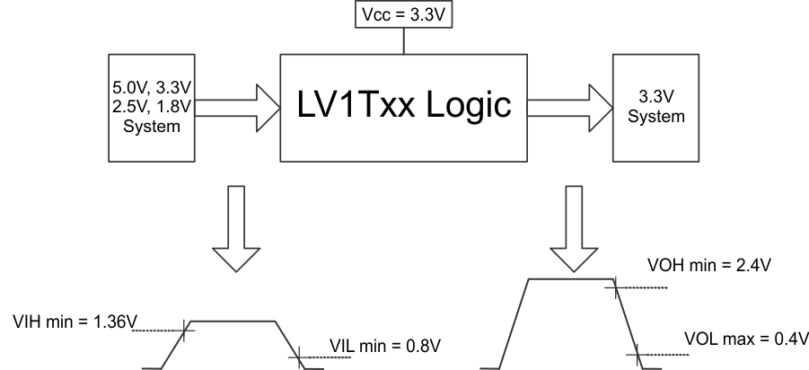
The SN74LV1T125 is a single buffer gate with reduced input thresholds to support voltage translation applications.
Package Information
| PART NUMBER | PACKAGE(1) | PACKAGE SIZE(2) | BODY SIZE(3) |
|---|---|---|---|
| SN74LV1T125 | DBV (SOT-23, 5) | 2.90mm × 2.8mm | 2.9mm x 1.6mm |
| DCK (SC70, 5) | 2.00mm × 2.1mm | 2mm × 1.25mm |
(1) For more information, see Section
12.
(2) The package size (length × width)
is a nominal value and includes pins, where applicable.
(3) The body size (length x width) is
a nominal value and does not include pins.

 Switching
Thresholds for 1.8V to 3.3V Translation