SCLS949 august 2023 SN74LV595B-EP
PRODUCTION DATA
- 1
- 1 Features
- 2 Applications
- 3 Description
- 4 Revision History
- 5 Pin Configuration and Functions
-
6 Specifications
- 6.1 Absolute Maximum Ratings
- 6.2 ESD Ratings
- 6.3 Recommended Operating Conditions
- 6.4 Thermal Information
- 6.5 Electrical Characteristics
- 6.6 Timing Requirements, VCC = 2.5 V ± 0.2 V
- 6.7 Timing Requirements, VCC = 3.3 V ± 0.3 V
- 6.8 Timing Requirements, VCC = 5 V ± 0.5 V
- 6.9 Switching Characteristics, VCC = 2.5 V ± 0.2 V
- 6.10 Switching Characteristics, VCC = 3.3 V ± 0.3 V
- 6.11 Switching Characteristics, VCC = 5 V ± 0.5 V
- 6.12 Noise Characteristics
- 6.13 Operating Characteristics
- 6.14 Typical Characteristics
- 7 Parameter Measurement Information
- 8 Detailed Description
- 9 Application and Implementation
- 10Device and Documentation Support
- 11Mechanical, Packaging, and Orderable Information
Package Options
Mechanical Data (Package|Pins)
- PW|16
Thermal pad, mechanical data (Package|Pins)
Orderable Information
6.8 Timing Requirements, VCC = 5 V ± 0.5 V
over operating free-air temperature range (unless otherwise noted)
| TA = 25°C | TA = −55°C TO 125°C | UNIT | |||||
|---|---|---|---|---|---|---|---|
| MIN | MAX | MIN | MAX | ||||
| tw | Pulse duration | SRCLK high or low | 5 | 6 | ns | ||
| RCLK high or low | 5 | 6 | |||||
| SRCLR low | 5.2 | 6.2 | |||||
| tsu | Setup time | SER before SRCLK↑ | 3 | 4 | ns | ||
| SRCLK↑ before RCLK↑(1) | 5 | 6 | |||||
| SRCLR low before RCLK↑ | 5 | 6 | |||||
| SRCLR high (inactive) before SRCLK↑ | 2.5 | 3.5 | |||||
| th | Hold time | SER after SRCLK↑ | 2 | 3 | ns | ||
(1) This setup time allows the storage register to receive stable data from the shift register. The clocks can be tied together, in which case the shift register is one clock pulse ahead of the storage register.
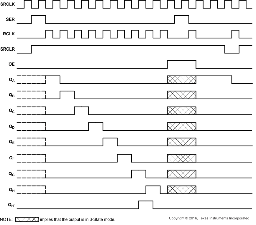
 Figure 6-1 Timing Diagram