SCES636B AUGUST 2005 – April 2015 SN74LVC16T245
PRODUCTION DATA.
- 1 Features
- 2 Applications
- 3 Description
- 4 Revision History
- 5 Description (continued)
- 6 Pin Configuration and Functions
-
7 Specifications
- 7.1 Absolute Maximum Ratings
- 7.2 ESD Ratings
- 7.3 Recommended Operating Conditions
- 7.4 Thermal Information
- 7.5 Electrical Characteristics
- 7.6 Switching Characteristics: VCCA = 1.8 V ±0.15 V
- 7.7 Switching Characteristics: VCCA = 2.5 V ±0.2 V
- 7.8 Switching Characteristics: VCCA = 3.3 V ±0.3 V
- 7.9 Switching Characteristics: VCCA = 5 V ±0.5 V
- 7.10 Operating Characteristics
- 7.11 Typical Characteristics
- 8 Parameter Measurement Information
- 9 Detailed Description
- 10Application and Implementation
- 11Power Supply Recommendations
- 12Layout
- 13Device and Documentation Support
- 14Mechanical, Packaging, and Orderable Information
Package Options
Refer to the PDF data sheet for device specific package drawings
Mechanical Data (Package|Pins)
- DGG|48
- DL|48
- DGV|48
Thermal pad, mechanical data (Package|Pins)
Orderable Information
10 Application and Implementation
NOTE
Information in the following applications sections is not part of the TI component specification, and TI does not warrant its accuracy or completeness. TI’s customers are responsible for determining suitability of components for their purposes. Customers should validate and test their design implementation to confirm system functionality.
10.1 Application Information
The SN74LVC16T245 device can be used in level-shifting applications for interfacing devices and addressing mixed voltage incompatibility. The SN74LVC16T245 device is ideal for data transmission where direction is different for each channel.
10.1.1 Enable Times
Calculate the enable times for the SN74LV16T245 using the following formulas:
In a bidirectional application, these enable times provide the maximum delay from the time the DIR bit is switched until an output is expected. For example, if the SN74LVC16T245 initially is transmitting from A to B, then the DIR bit is switched; the B port of the device must be disabled before presenting it with an input. After the B port has been disabled, an input signal applied to it appears on the corresponding A port after the specified propagation delay.
10.2 Typical Application
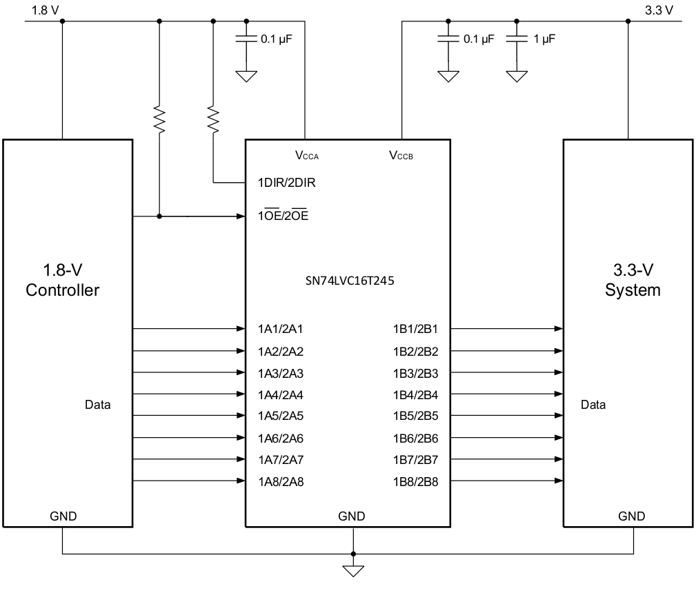
 Figure 4. Typical Application Schematic
10.2.1 Design Requirements
This device uses drivers which are enabled depending on the state of the DIR pin. The designer must know the intended flow of data and take care not to violate any of the high or low logic levels. It is important that unused data inputs not be floating, as this can cause excessive internal leakage on the input CMOS structure. Make sure to tie any unused input and output ports directly to ground. For this design example, use the parameters listed in Table 2.
Table 2. Design Parameters
| DESIGN PARAMETERS | EXAMPLE VALUE | |||
|---|---|---|---|---|
| Input voltage range | 1.65 V to 5.5 V | |||
| Output voltage | 1.65 V to 5.5 V | |||
10.2.2 Detailed Design Procedure
To begin the design process, determine the following:
- Input voltage range
- Use the supply voltage of the device that is driving the SN74LVC16T245 device to determine the input voltage range. For a valid logic high the value must exceed the VIH of the input port. For a valid logic low the value must be less than the VIL of the input port.
- Output voltage range
- Use the supply voltage of the device that the SN74LVC16T245 device is driving to determine the output voltage range.
10.2.3 Application Curve
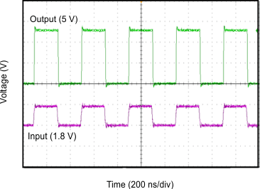
 Figure 5. Translation Up (1.8 V to 5 V) at 2.5 MHz