SCES636B AUGUST 2005 – April 2015 SN74LVC16T245
PRODUCTION DATA.
- 1 Features
- 2 Applications
- 3 Description
- 4 Revision History
- 5 Description (continued)
- 6 Pin Configuration and Functions
-
7 Specifications
- 7.1 Absolute Maximum Ratings
- 7.2 ESD Ratings
- 7.3 Recommended Operating Conditions
- 7.4 Thermal Information
- 7.5 Electrical Characteristics
- 7.6 Switching Characteristics: VCCA = 1.8 V ±0.15 V
- 7.7 Switching Characteristics: VCCA = 2.5 V ±0.2 V
- 7.8 Switching Characteristics: VCCA = 3.3 V ±0.3 V
- 7.9 Switching Characteristics: VCCA = 5 V ±0.5 V
- 7.10 Operating Characteristics
- 7.11 Typical Characteristics
- 8 Parameter Measurement Information
- 9 Detailed Description
- 10Application and Implementation
- 11Power Supply Recommendations
- 12Layout
- 13Device and Documentation Support
- 14Mechanical, Packaging, and Orderable Information
Package Options
Refer to the PDF data sheet for device specific package drawings
Mechanical Data (Package|Pins)
- DGG|48
- DL|48
- DGV|48
Thermal pad, mechanical data (Package|Pins)
Orderable Information
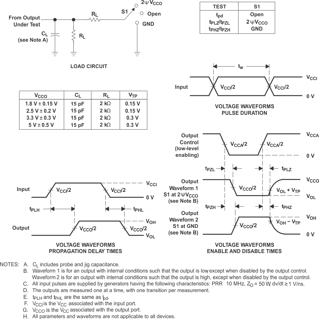
8 Parameter Measurement Information
 Figure 3. Load Circuit and Voltage Waveforms