SCES223T April 1999 – October 2014 SN74LVC1G125
PRODUCTION DATA.
- 1 Features
- 2 Applications
- 3 Description
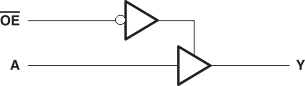
- 4 Simplified Schematic
- 5 Revision History
- 6 Pin Configuration and Functions
-
7 Specifications
- 7.1 Absolute Maximum Ratings
- 7.2 Handling Ratings
- 7.3 Recommended Operating Conditions
- 7.4 Thermal Information
- 7.5 Electrical Characteristics
- 7.6 Switching Characteristics, CL = 15 pF
- 7.7 Switching Characteristics, -40°C to 85°C
- 7.8 Switching Characteristics, -40°C to 125°C
- 7.9 Operating Characteristics
- 7.10 Typical Characteristics
- 8 Parameter Measurement Information
- 9 Detailed Description
- 10Application and Implementation
- 11Power Supply Recommendations
- 12Layout
- 13Device and Documentation Support
- 14Mechanical, Packaging, and Orderable Information
9 Detailed Description
9.1 Overview
The SN74LVC1G125 device contains one buffer gate device with output enable control and performs the Boolean function Y = A. This device is fully specified for partial-power-down applications using Ioff. The Ioff circuitry disables the outputs, preventing damaging current backflow through the device when it is powered down.
To ensure the high-impedance state during power up or power down, OE should be tied to VCC through a pullup resistor; the minimum value of the resistor is determined by the current-sinking capability of the driver.
The DPW package technology is a major breakthrough in IC packaging. Its tiny 0.64 mm square footprint saves significant board space over other package options while still retaining the traditional manufacturing friendly lead pitch of 0.5 mm.
9.2 Functional Block Diagram
9.3 Feature Description
- Wide operating voltage range
- Operates from 1.65 V to 5.5 V
- Allows down voltage translation
- Inputs accept voltages to 5.5 V
- Ioff feature allows voltages on the inputs and outputs, when VCC is 0 V
9.4 Device Functional Modes
Table 1. Function Table
| INPUTS | OUTPUT Y |
|
|---|---|---|
| OE | A | |
| L | H | H |
| L | L | L |
| H | X | Z |