SCES416N December 2002 – January 2017 SN74LVC1G97
PRODUCTION DATA.
- 1 Features
- 2 Applications
- 3 Description
- 4 Revision History
- 5 Pin Configuration and Functions
- 6 Specifications
- 7 Parameter Measurement Information
- 8 Detailed Description
- 9 Application and Implementation
- 10Power Supply Recommendations
- 11Layout
- 12Device and Documentation Support
- 13Mechanical, Packaging, and Orderable Information
Package Options
Mechanical Data (Package|Pins)
Thermal pad, mechanical data (Package|Pins)
- DRY|6
Orderable Information
8 Detailed Description
8.1 Overview
This configurable multiple-function gate is designed for 1.65-V to 5.5-V VCC operation.
The SN74LVC1G97 device features configurable multiple functions. The output state is determined by eight patterns of 3-bit input. The user can choose variations of common logic functions, like AND, OR, and NOT. All inputs can be connected to VCC or GND.
This device functions as an independent gate, but because of Schmitt action, it may have different input threshold levels for positive-going (VT+) and negative-going (VT–) signals.
This device is fully-specified for partial-power-down applications using Ioff. The Ioff circuitry disables the outputs, preventing damaging current backflow through the device when it is powered down.
8.2 Functional Block Diagram

8.3 Feature Description
The SN74LVC1G97 device has a wide operating VCC range of 1.65 V to 5.5 V, which allows use in a broad range of systems. The 5.5-V I/Os allow down translation and also allow voltages at the inputs when VCC = 0 V.
8.4 Device Functional Modes
Table 1 shows the functional modes of SN74LVC1G97.
Table 1. Function Table
| INPUTS | OUTPUT | ||
|---|---|---|---|
| In2 | In1 | In0 | Y |
| L | L | L | L |
| L | L | H | L |
| L | H | L | H |
| L | H | H | H |
| H | L | L | L |
| H | L | H | H |
| H | H | L | L |
| H | H | H | H |
Table 2. Function Selection Table
| LOGIC FUNCTION | FIGURE NUMBER |
|---|---|
| 2-to-1 data selector | Figure 3 |
| 2-input AND gate | Figure 4 |
| 2-input OR gate with one inverted input | Figure 5 |
| 2-input NAND gate with one inverted input | Figure 5 |
| 2-input AND gate with one inverted input | Figure 6 |
| 2-input NOR gate with one inverted input | Figure 6 |
| 2-input OR gate | Figure 7 |
| Inverter | Figure 8 |
| Noninverted buffer | Figure 9 |
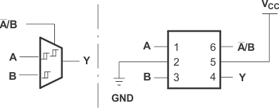 Figure 3. 2-to-1 Data Selector
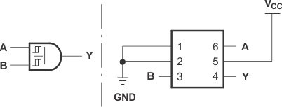 Figure 4. 2-Input AND Gate
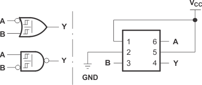 Figure 5. 2-Input OR Gate With One Inverted Input
2-Input NAND Gate With One Inverted Input
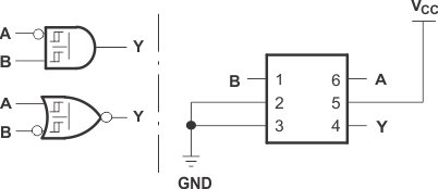 Figure 6. 2-Input AND Gate With One Inverted Input
2-Input NOR Gate With One Inverted Input
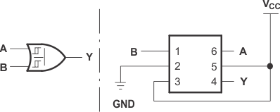 Figure 7. 2-Input OR Gate
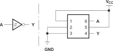 Figure 8. Inverter
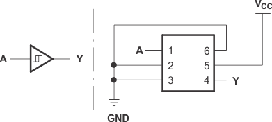 Figure 9. Noninverted Buffer