SCAS293L January 1993 – July 2014 SN74LVC240A
PRODUCTION DATA.
- 1 Features
- 2 Applications
- 3 Simplified Schematic
- 4 Revision History
- 5 Pin Configuration and Functions
- 6 Specifications
- 7 Detailed Description
- 8 Application and Implementation
- 9 Power Supply Recommendations
- 10Layout
- 11Device and Documentation Support
Package Options
Refer to the PDF data sheet for device specific package drawings
Mechanical Data (Package|Pins)
- DGV|20
- DB|20
- NS|20
- DGS|20
- DW|20
- PW|20
Thermal pad, mechanical data (Package|Pins)
Orderable Information
8 Application and Implementation
8.1 Application Information
The SN74LVC240A device is a high drive CMOS device that can be used for a multitude of bus-interface type applications where the data needs to be retained or latched. It can produce 24 mA of drive current at 3.3 V making it ideal for driving multiple outputs and also good for high-speed applications up to 100 Mhz. The inputs are 5.5 V tolerant allowing it to translate down to VCC.
8.2 Typical Application
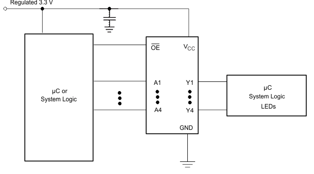 Figure 4. Typical Application Diagram
8.2.1 Design Requirements
This device uses CMOS technology and has balanced output drive. Care should be taken to avoid bus contention because it can drive currents that would exceed maximum limits. The high drive will also create fast edges into light loads; therefore, routing and load conditions should be considered to prevent ringing.
8.2.2 Detailed Design Procedure
- Recommended Input Conditions
- Rise time and fall time specs: See (Δt/ΔV) in the Recommended Operating Conditions table.
- Specified high and low levels: See (VIH and VIL) in the Recommended Operating Conditions table.
- Inputs are overvoltage tolerant allowing them to go as high as 5.5 V at any valid VCC.
- Recommend Output Conditions
- Load currents should not exceed 25 mA per output and 50 mA total for the part.
- Outputs should not be pulled above VCC.
8.2.3 Application Curves
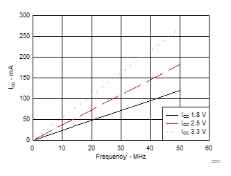 Figure 5. ICC vs Frequency