SCAS294P January 1993 – May 2024 SN54LVC257A , SN74LVC257A
PRODUCTION DATA
- 1
- 1 Features
- 2 Applications
- 3 Description
- 4 Pin Configuration and Functions
- 5 Specifications
- 6 Parameter Measurement Information
- 7 Detailed Description
- Application and Implementation
- 8 Device and Documentation Support
- 9 Revision History
- 10Mechanical, Packaging, and Orderable Information
Package Options
Mechanical Data (Package|Pins)
Thermal pad, mechanical data (Package|Pins)
- RGY|16
Orderable Information
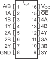
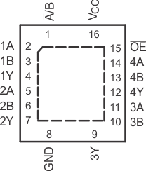
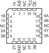
4 Pin Configuration and Functions
 Figure 4-1 D, DB, NS, J, W, or PW Package;16-Pin SOIC, SSOP, SO, CDIP, CFP, or
TSSOP(Top View)
 Figure 4-2 BQB or RGY Package;16-Pin WQFN or VQFN with Exposed Thermal
Pad(Top View)
 Figure 4-3 FK Package,20-Pin LCCCTop View
| PIN | I/O | DESCRIPTION | ||
|---|---|---|---|---|
| NAME | SOIC, SSOP, SO, CDIP, CFP, TSSOP, WQFN, or VQFN | LCCC | ||
| A/B | 1 | 2 | I | Select Pin, Low selects A, High selects B |
| 1A | 2 | 3 | I/O | Multiplexer Signal Input |
| 1B | 3 | 4 | I/O | Multiplexer Signal Input |
| 1Y | 4 | 5 | I/O | Multiplexer Output |
| 2A | 5 | 7 | I/O | Multiplexer Signal Input |
| 2B | 6 | 8 | I/O | Multiplexer Signal Input |
| 2Y | 7 | 9 | I/O | Multiplexer Output |
| 3A | 11 | 14 | I/O | Multiplexer Signal Input |
| 3B | 10 | 13 | I/O | Multiplexer Signal Input |
| 3Y | 9 | 12 | I/O | Multiplexer Output |
| 4A | 14 | 18 | I/O | Multiplexer Signal Input |
| 4B | 13 | 17 | I/O | Multiplexer Signal Input |
| 4Y | 12 | 15 | I/O | Multiplexer Output |
| GND | 8 | 10 | — | Ground |
| NC(1) | — | 1, 6, 11, 16 | — | No connect |
| OE | 15 | 19 | I/O | Active low Output enable |
| VCC | 16 | 20 | — | Power pin |
(1) NC – no internal connection