SCAS375J March 1994 – December 2022 SN74LVC4245A
PRODUCTION DATA
- 1 Features
- 2 Applications
- 3 Description
- 4 Revision History
- 5 Pin Configuration and Functions
-
6 Specifications
- 6.1 Absolute Maximum Ratings
- 6.2 Absolute Maximum Ratings
- 6.3 ESD Ratings
- 6.4 Recommended Operating Conditions
- 6.5 Recommended Operating Conditions
- 6.6 Thermal Information
- 6.7 Electrical Characteristics
- 6.8 Electrical Characteristics
- 6.9 Switching Characteristics
- 6.10 Operating Characteristics
- 6.11 Typical Characteristics
- 7 Parameter Measurement Information
- 8 Detailed Description
- 9 Application and Implementation
- 10Power Supply Recommendations
- 11Layout
- 12Device and Documentation Support
- 13Mechanical, Packaging, and Orderable Information
Package Options
Mechanical Data (Package|Pins)
Thermal pad, mechanical data (Package|Pins)
- DW|24
Orderable Information
3 Description
This 8-bit (octal) noninverting bus transceiver contains two separate supply rails; B port has VCCB, which is set at 3.3 V, and A port has VCCA, which is set at 5 V. This allows for translation from a 3.3-V to a 5-V environment, and vice versa.
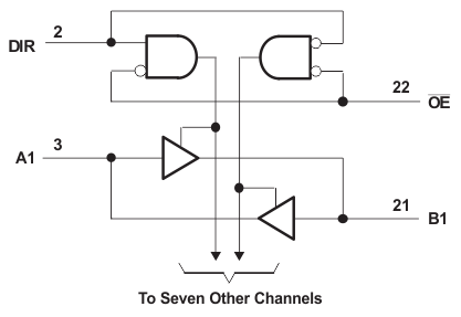
The SN74LVC4245A device is designed for asynchronous communication between data buses. The device transmits data from the A bus to the B bus or from the B bus to the A bus, depending on the logic level at the direction-control (DIR) input. The output-enable (OE) input can be used to disable the device so the buses are effectively isolated. The control circuitry (DIR, OE) is powered by VCCA.
The SN74LVC4245A device terminal out allows the designer to switch to a normal all-3.3-V or all-5-V 20-terminal SN74LVC4245 device without board re-layout. The designer uses the data paths for pins 2–11 and 14–23 of the SN74LVC4245A device to align with the conventional '245 terminal out.
| PART NUMBER | PACKAGE | BODY SIZE (NOM) |
|---|---|---|
| SN74LVC4245A | DB (SSOP, 24) | 8.20 mm × 5.30 mm |
| DW (SOIC, 24) | 15.40 mm × 7.50 mm | |
| PW (TSSOP, 24) | 7.80 mm × 4.40 mm |
 Simplified Schematic