SCLS999 March   2024 SN74LVC7266A-Q1

PRODUCTION DATA  

  1.   1
  2. Features
  3. Applications
  4. Description
  5. Pin Configuration and Functions
  6. Specifications
    1. 5.1 Absolute Maximum Ratings
    2. 5.2 ESD Ratings
    3. 5.3 Recommended Operating Conditions
    4. 5.4 Thermal Information
    5. 5.5 Electrical Characteristics
    6. 5.6 Switching Characteristics
    7. 5.7 Noise Characteristics
    8. 5.8 Typical Characteristics
  7. Parameter Measurement Information
  8. Detailed Description
    1. 7.1 Overview
    2. 7.2 Functional Block Diagram
    3. 7.3 Feature Description
      1. 7.3.1 Balanced CMOS Push-Pull Outputs
      2. 7.3.2 Standard CMOS Inputs
      3. 7.3.3 Clamp Diode Structure
      4. 7.3.4 Wettable Flanks
    4. 7.4 Device Functional Modes
  9. Application and Implementation
    1. 8.1 Application Information
    2. 8.2 Typical Application
      1. 8.2.1 Design Requirements
        1. 8.2.1.1 Power Considerations
        2. 8.2.1.2 Input Considerations
        3. 8.2.1.3 Output Considerations
      2. 8.2.2 Detailed Design Procedure
      3. 8.2.3 Application Curves
    3. 8.3 Power Supply Recommendations
    4. 8.4 Layout
      1. 8.4.1 Layout Guidelines
      2. 8.4.2 Layout Example
  10. Device and Documentation Support
    1. 9.1 Documentation Support
      1. 9.1.1 Related Documentation
    2. 9.2 Receiving Notification of Documentation Updates
    3. 9.3 Support Resources
    4. 9.4 Trademarks
    5. 9.5 Electrostatic Discharge Caution
    6. 9.6 Glossary
  11. 10Revision History
  12. 11Mechanical, Packaging, and Orderable Information

Package Options

Refer to the PDF data sheet for device specific package drawings

Mechanical Data (Package|Pins)
  • PW|14
  • BQA|14
Thermal pad, mechanical data (Package|Pins)
Orderable Information

Description

The SN74LVC7266A-Q1 contains four independent 2-input XNOR gates. Each gate performs the Boolean function Y = A ⊕ B in positive logic.

Package Information
PART NUMBERPACKAGE(1)PACKAGE SIZE(2)BODY SIZE (NOM)(3)
SN74LVC7266A-Q1BQA (WQFN, 14)3mm × 2.5mm3mm × 2.5mm
PW (TSSOP, 14)5mm × 6.4mm5mm × 4.4mm
For more information, see Section 11.
The package size (length × width) is a nominal value and includes pins, where applicable.
The body size (length × width) is a nominal value and does not include pins.
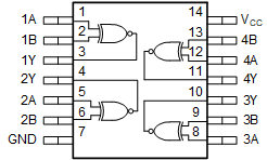
GUID-EF3D367D-0EBD-460E-AB80-15EAF17A702B-low.gif Logic Diagram