SCES495C October 2003 – June 2014 SN74LVCH16245A
PRODUCTION DATA.
- 1 Features
- 2 Applications
- 3 Description
- 4 Simplified Schematic
- 5 Revision History
- 6 Pin Configuration and Functions
- 7 Specifications
- 8 Parameter Measurement Information
- 9 Detailed Description
- 10Application and Implementation
- 11Power Supply Recommendations
- 12Layout
- 13Device and Documentation Support
- 14Mechanical, Packaging, and Orderable Information
Package Options
Mechanical Data (Package|Pins)
Thermal pad, mechanical data (Package|Pins)
Orderable Information
10 Application and Implementation
10.1 Application Information
The SN74LVC16245A device is a 16-bit bidirectional transceiver. This device can be used as two 8-bit transceivers or one 16-bit transceiver. It allows data transmission from the A bus to the B bus or from the B bus to the A bus, depending on the logic level at the direction-control (DIR) input. The output-enable (OE) input can be used to disable the device so that the buses are effectively isolated. The device has 5.5 V tolerant inputs at any valid VCC. This allows it to be used in multi-power systems, and it can be used for down translation.
10.2 Typical Application
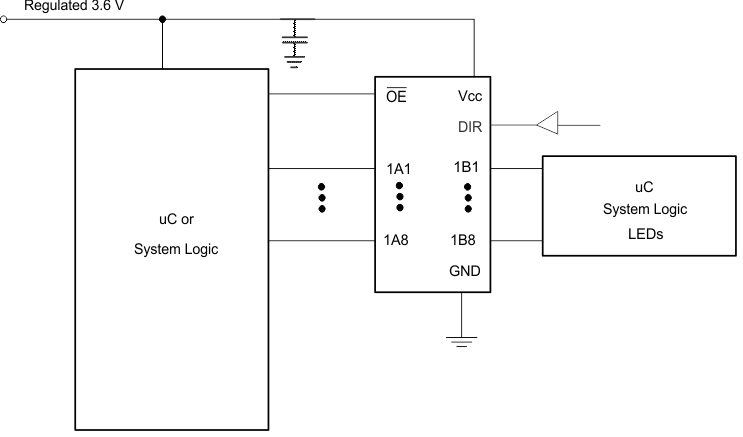 Figure 5. Typical Application Diagram
10.2.1 Design Requirements
This device uses CMOS technology and has balanced output drive. Care should be taken to avoid bus contention because it can drive currents that would exceed maximum limits. The high drive will also create fast edges into light loads; therefore, routing and load conditions should be considered to prevent ringing.
10.2.2 Detailed Design Procedure
- Recommended Input Conditions
- Rise time and fall time specs: See (Δt/ΔV) in the Recommended Operating Conditions table.
- Specified high and low levels: See (VIH and VIL) in the Recommended Operating Conditions table.
- Inputs are overvoltage tolerant allowing them to go as high as 5.5 V at any valid VCC.
- Recommend Output Conditions
- Load currents should not exceed 25 mA per output and 50 mA total for the part.
- Outputs should not be pulled above VCC.
10.2.3 Application Curves
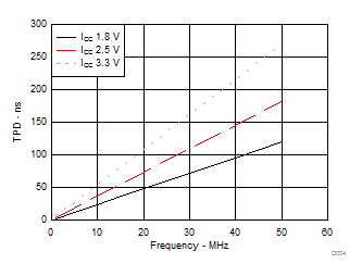 Figure 6. ICC vs Frequency