SCAS582Q November 1996 – October 2014 SN74LVCHR16245A
PRODUCTION DATA.
- 1 Features
- 2 Applications
- 3 Simplified Schematic
- 4 Revision History
- 5 Pin Configuration and Functions
- 6 Specifications
- 7 Detailed Description
- 8 Application and Implementation
- 9 Power Supply Recommendations
- 10Layout
- 11Device and Documentation Support
Package Options
Refer to the PDF data sheet for device specific package drawings
Mechanical Data (Package|Pins)
- DGG|48
- DL|48
- DGV|48
Thermal pad, mechanical data (Package|Pins)
Orderable Information
7 Detailed Description
7.1 Overview
This 16-bit (dual-octal) noninverting bus transceiver is designed for 1.65-V to 3.6-V VCC operation.
The SN74LVCHR16245A device is designed for asynchronous communication between data buses. The control-function implementation minimizes external-timing requirements.
This device can be used as two 8-bit transceivers or one 16-bit transceiver. It allows data transmission from the A bus to the B bus or from the B bus to the A bus, depending on the logic level at the direction-control (DIR) input. The output-enable (OE) input can disable the device so that the buses are effectively isolated.
All outputs, which are designed to sink up to 12 mA, include equivalent 26-Ω series resistors to reduce overshoot and undershoot.
Inputs can be driven from either 3.3-V or 5-V devices. This feature allows the use of this device as a translator in a mixed 3.3-V/5-V system environment.
To ensure the high-impedance state during power up or power down, OE should be tied to VCC through a pullup resistor; the minimum value of the resistor is determined by the current-sinking capability of the driver.
This device is fully specified for partial-power-down applications using Ioff. The Ioff circuitry disables the outputs, preventing damaging current backflow through the device when it is powered down.
Active bus-hold circuitry is provided to hold unused or floating data inputs at a valid logic level. Use of pullup or pulldown resistors with the bus-hold circuitry is not recommended. The bus-hold circuitry is part of the input circuit and is not disabled by OE or DIR.
7.2 Functional Block Diagram
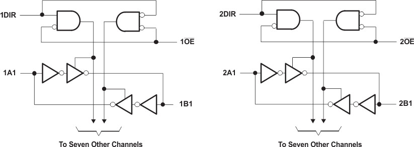 Figure 4. Logic Diagram (Positive Logic)
7.3 Feature Description
- Wide operating voltage range
- Operates from 1.65 V to 3.6 V
- Allows down voltage translation
- Inputs accept voltages to 5.5 V
- Ioff feature
- Allows voltages on the inputs and outputs when VCC is 0 V
- All outputs have equivalent 26-Ω series resistors, so no external resistors are required
- Bus hold on data inputs eliminates the need for external pullup or pulldown resistors
7.4 Device Functional Modes
Table 3. Function Table(1)
(Each 8-bit Section)
| CONTROL INPUTS | OUTPUT CIRCUITS | OPERATION | ||
|---|---|---|---|---|
| OE | DIR | A PORT | B PORT | |
| L | L | Enabled | Hi-Z | B data to A bus |
| L | H | Hi-Z | Enabled | A data to B bus |
| H | X | Hi-Z | Hi-Z | Isolation |