SCES274I May 1999 – October 2014 SN74LVCZ244A
PRODUCTION DATA.
- 1 Features
- 2 Applications
- 3 Description
- 4 Simplified Schematic
- 5 Revision History
- 6 Pin Configuration and Functions
- 7 Specifications
- 8 Parameter Measurement Information
- 9 Detailed Description
- 10Application and Implementation
- 11Power Supply Recommendations
- 12Layout
- 13Device and Documentation Support
- 14Mechanical, Packaging, and Orderable Information
Package Options
Refer to the PDF data sheet for device specific package drawings
Mechanical Data (Package|Pins)
- DB|20
- NS|20
- DGS|20
- DW|20
- PW|20
Thermal pad, mechanical data (Package|Pins)
Orderable Information
10 Application and Implementation
NOTE
Information in the following applications sections is not part of the TI component specification, and TI does not warrant its accuracy or completeness. TI’s customers are responsible for determining suitability of components for their purposes. Customers should validate and test their design implementation to confirm system functionality.
10.1 Application Information
Inputs can be driven from either 3.3-V or 5-V devices. This feature allows the use of this device as a translator in a mixed 3.3-V/5-V system environment.
The SN74LVCZ244A device is fully specified for partial-power-down applications using Ioff. The Ioff circuitry disables the outputs, preventing damaging current backflow through the device when it is powered down. This device is fully specified for hot-insertion applications using Ioff and power-up 3-state. The Ioff circuitry disables the outputs, preventing damaging current backflow through the device when it is powered down.
The power-up 3-state circuitry places the outputs in the high-impedance state during power up and power down, which prevents driver conflict. To ensure the high-impedance state during power up or power down, OE should be tied to VCC through a pullup resistor; the minimum value of the resistor is determined by the current-sinking capability of the driver.
10.2 Typical Application
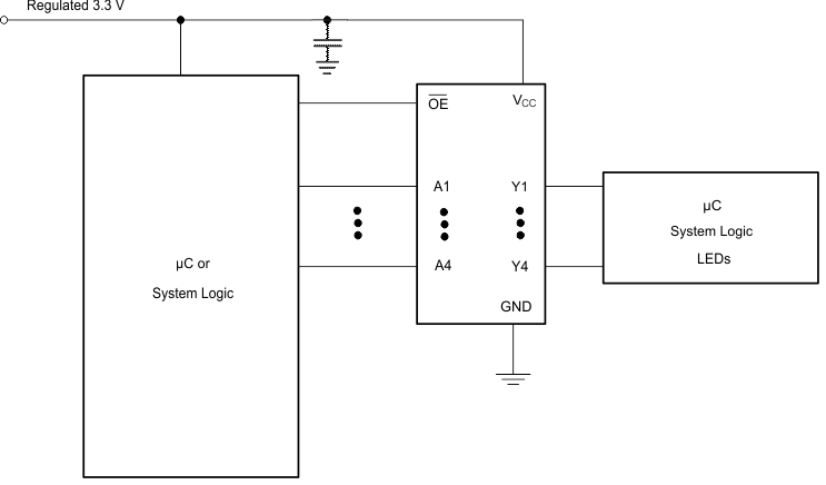 Figure 4. Typical Application Schematic
10.2.1 Design Requirements
This device uses CMOS technology and has balanced output drive. Care should be taken to avoid bus contention, because it can drive currents that would exceed maximum limits. The high drive will also create fast edges into light loads; therefore, routing and load conditions should be considered to prevent ringing.
10.2.2 Detailed Design Procedure
- Recommended Input Conditions:
- For rise time and fall time specifications, see Δt/ΔV in the Recommended Operating Conditions table.
- For specified high and low levels, see VIH and VIL in the Recommended Operating Conditions table.
- Inputs are overvoltage tolerant allowing them to go as high as 5.5 V at any valid VCC.
- Recommend Output Conditions:
- Load currents should not exceed 50 mA per output and 100 mA total for the part.
- Outputs should not be pulled above VCC.
10.2.3 Application Curves
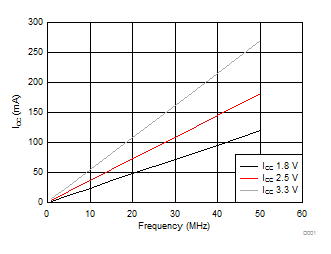 Figure 5. ICC vs Frequency