SLLS145D October 1990 – October 2023 SN65175 , SN75175
PRODUCTION DATA
- 1
- 1 Features
- 2 Applications
- 3 Description
- 4 Pin Configuration and Functions
- 5 Specifications
- 6 Parameter Measurement Information
- 7 Detailed Description
- 8 Application and Implementation
- 9 Device and Documentation Support
- 10Revision History
- 11Mechanical, Packaging, and Orderable Information
Package Options
Refer to the PDF data sheet for device specific package drawings
Mechanical Data (Package|Pins)
- NS|16
- N|16
- D|16
Thermal pad, mechanical data (Package|Pins)
- D|16
Orderable Information
3 Description
The SN65175 and SN75175 are monolithic quadruple differential line receivers with 3-state outputs. They are designed to meet the requirements of ANSI Standards EIA/TIA-422-B, RS-423-B, and RS-485, and several ITU recommendations. These standards are for balanced multipoint bus transmission at rates up to 10 megabits per second. Each of the two pairs of receivers has a common active-high enable.
The receivers feature high input impedance, input hysteresis for increased noise immunity, and input sensitivity of ±200 mV over a common-mode input voltage range of ±12 V. The SN65175 and SN75175 are designed for optimum performance when used with the SN75172 or SN75174 quadruple differential line drivers.
The SN65175 is characterized for operation from −40°C to 85°C. The SN75175 is characterized for operation from 0°C to 70°C.
| PART NUMBER | PACKAGE(1) | PACKAGE SIZE(2) |
|---|---|---|
| SN65175 | D (SOIC, 16) | 9.9 mm × 6 mm |
| SN75175 | N (PDIP, 16) | 19.3 mm × 9.4 mm |
| D (SOIC, 16) | 9.9 mm × 6 mm | |
| NS (SOP, 16) | 10.2 mm × 7.8 mm |
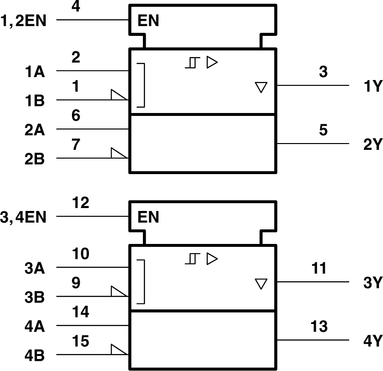
 Logic Symbol (1)
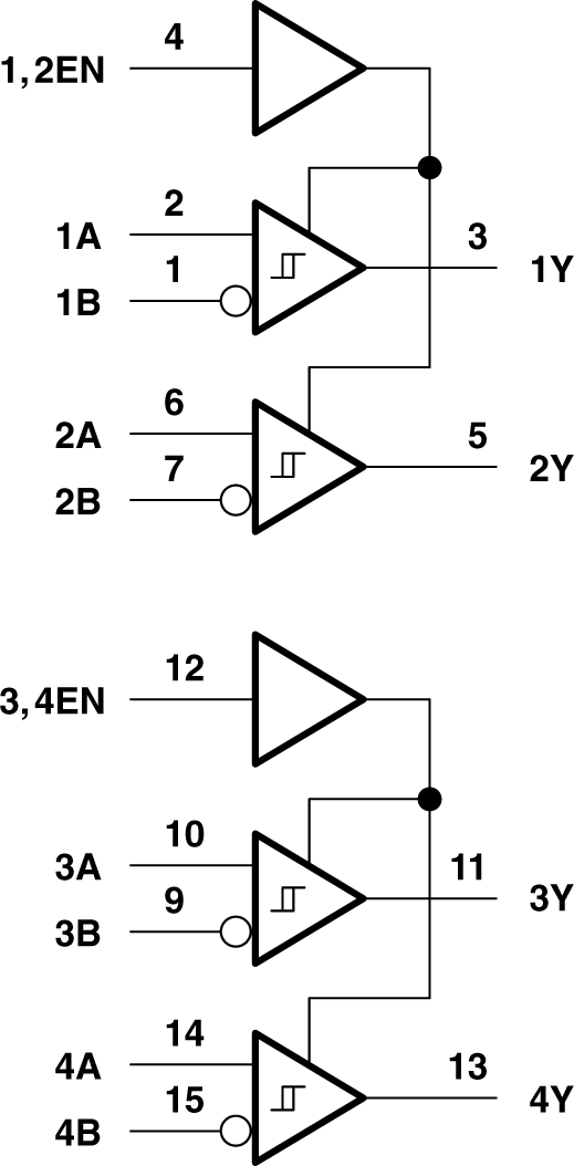
 Logic Diagram (Positive Logic)