SLRS007C November 1986 – January 2015 SN754410
PRODUCTION DATA.
- 1 Features
- 2 Applications
- 3 Description
- 4 Simplified Schematic
- 5 Revision History
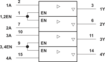
- 6 Pin Configuration and Functions
- 7 Specifications
- 8 Parameter Measurement Information
- 9 Detailed Description
- 10Application and Implementation
- 11Power Supply Recommendations
- 12Layout
- 13Device and Documentation Support
- 14Mechanical, Packaging, and Orderable Information
Package Options
Refer to the PDF data sheet for device specific package drawings
Mechanical Data (Package|Pins)
- NE|16
Thermal pad, mechanical data (Package|Pins)
Orderable Information
9 Detailed Description
9.1 Overview
The SN754410 is a quadruple high-current half-H driver designed to provide bidirectional drive currents up to 1 A at voltages from 4.5 V to 36 V. The device is designed to drive inductive loads such as relays, solenoids, DC and bipolar stepping motors, as well as other high-current/high-voltage loads in positive-supply applications. All inputs are compatible with TTL and low-level CMOS logic. Each output (Y) is a complete totem-pole driver with a Darlington transistor sink and a pseudo-Darlington source. Drivers are enabled in pairs with drivers 1 and 2 enabled by 1,2EN and drivers 3 and 4 enabled by 3,4EN. When an enable input is high, the associated drivers are enabled and their outputs become active and in phase with their inputs. When the enable input is low, those drivers are disabled and their outputs are off and in a high-impedance state. With the proper data inputs, each pair of drivers form a full-H (or bridge) reversible drive suitable for solenoid or motor applications.
A separate supply voltage (VCC1) is provided for the logic input circuits to minimize device power dissipation. Supply voltage VCC2 is used for the output circuits. The SN754410 is designed for operation from −40°C to 85°C.
9.2 Functional Block Diagram
9.3 Feature Description
9.3.1 High Current, High Voltage Outputs
Four high current and high voltage outputs feature clamp diodes for inductive load driving.
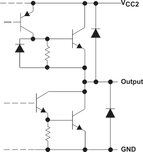 Figure 5. Typical of All Outputs
9.3.2 TTL Compatible Inputs
Data inputs and enable inputs are compatible with TTL. 3.3-V CMOS logic is also acceptable, however open or high impedance input voltage can approach VCC1 voltage.
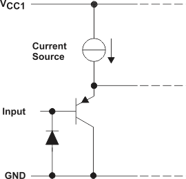 Figure 6. Equivalent of Each Input