SLLS032C December 1987 – March 2024 SN75ALS191
PRODUCTION DATA
- 1
- 1 Features
- 2 Applications
- 3 Description
- 4 Pin Configuration and Functions
- 5 Specifications
- 6 Parameter Measurement Information
- 7 Detailed Description
- 8 Device and Documentation Support
- 9 Revision History
- 10Mechanical, Packaging, and Orderable Information
Package Options
Refer to the PDF data sheet for device specific package drawings
Mechanical Data (Package|Pins)
- D|8
- P|8
- PS|8
Thermal pad, mechanical data (Package|Pins)
- PS|8
Orderable Information
3 Description
The SN75ALS191 is a dual, high-speed, differential line driver designed to meet ANSI Standard EIA/TIA-422-B and ITU Recommendation V.11. The inputs are TTL- and CMOS-compatible and have input clamp diodes. Schottky-diode-clamped transistors minimize propagation delay time. This device operates from a single 5V power supply and is supplied in eight-pin packages.
The SN75ALS191 is characterized for operation from 0°C to 70°C.
Package Information
| PART NUMBER | PACKAGE(1) | PACKAGE SIZE(2) |
|---|---|---|
| SN75ALS191 | P (PDIP, 8) | 9.81mm × 9.43mm |
| D (SOIC, 8) | 4.9mm × 6mm | |
| PS (SOP, 8) | 6.2mm × 7.8mm |
(1) For more information, see Section 10.
(2) The package size (length × width) is a nominal value and includes pins, where applicable.
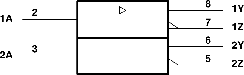 Logic Symbol(1)
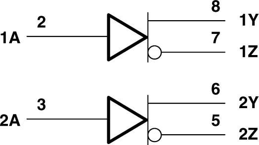 Logic Diagram (Positive Logic)
1. This
symbol is in accordance with ANSI/IEEE Std 91-1984 and IEC
Publication 617-12.