SLLS540C July   2002  – June 2021 SN65C3232 , SN75C3232

PRODUCTION DATA  

  1. Features
  2. Applications
  3. Description
  4. Revision History
  5. Pin Configuration and Functions
  6. Specifications
    1. 6.1  Absolute Maximum Ratings
    2. 6.2  ESD Ratings
    3. 6.3  Recommended Operating Conditions
    4. 6.4  Thermal Information
    5. 6.5  Electrical Characteristics
    6. 6.6  Driver Section - Electrical Characteristics
    7. 6.7  Switching Characteristics
    8. 6.8  Receiver Section - Electrical Characteristics
    9. 6.9  Switching Characteristics
    10. 6.10 Typical Characteristics
  7. Parameter Measurement Information
  8. Detailed Description
    1. 8.1 Overview
    2. 8.2 Functional Block Diagram
    3. 8.3 Feature Description
      1. 8.3.1 Power
      2. 8.3.2 RS232 Driver
      3. 8.3.3 RS232 Receiver
    4. 8.4 Device Functional Modes
      1. 8.4.1 VCC Powered by 3 V to 5.5 V
      2. 8.4.2 VCC Unpowered, VCC = 0 V
  9. Application and Implementation
    1. 9.1 Application Information
      1. 9.1.1 Typical Application
        1. 9.1.1.1 Design Requirements
        2. 9.1.1.2 Detailed Design Procedure
        3. 9.1.1.3 Application Performance Plots
  10. 10Layout
    1. 10.1 Layout Guidelines
    2. 10.2 Layout Example
  11. 11Device and Documentation Support
    1. 11.1 Documentation Support
      1. 11.1.1 Related Documentation
        1. 11.1.1.1 Related Links
    2. 11.2 Receiving Notification of Documentation Updates
    3. 11.3 Support Resources
    4. 11.4 Trademarks
    5. 11.5 Electrostatic Discharge Caution
    6. 11.6 Glossary
  12. 12Mechanical, Packaging, and Orderable Information

Package Options

Refer to the PDF data sheet for device specific package drawings

Mechanical Data (Package|Pins)
  • DB|16
  • DW|16
  • D|16
Thermal pad, mechanical data (Package|Pins)
Orderable Information

Typical Characteristics

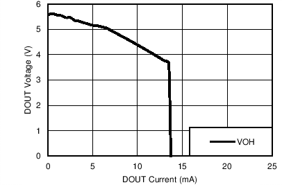
GUID-9289EEC8-1BA5-4809-85C6-2EDBB8F023C3-low.png
VCC = 3.3 V
Figure 6-1 DOUT VOH vs Load Current, Both Drivers Loaded
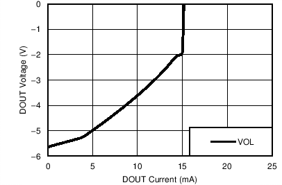
GUID-30BD73C4-F097-4D74-B565-255615D7B305-low.png
VCC = 3.3 V
Figure 6-2 DOUT VOL vs Load Current, Both Drivers Loaded