SLLSE81A March 2011 – March 2016 SN75LVCP600S
PRODUCTION DATA.
- 1 Features
- 2 Applications
- 3 Description
- 4 Revision History
- 5 Pin Configuration and Functions
- 6 Specifications
- 7 Parameter Measurement Information
- 8 Detailed Description
- 9 Application and Implementation
- 10Power Supply Recommendations
- 11Layout
- 12Device and Documentation Support
- 13Mechanical, Packaging, and Orderable Information
Package Options
Mechanical Data (Package|Pins)
- DSK|10
Thermal pad, mechanical data (Package|Pins)
- DSK|10
Orderable Information
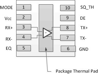
5 Pin Configuration and Functions
DSK Package
10-Pin (SON)
Top View

TI recommends soldering the package thermal pad to the ground plane for maximum thermal performance.
Pin Functions
| PIN | I/O TYPE | DESCRIPTION | |
|---|---|---|---|
| NO. | NAME | ||
| HIGH SPEED DIFFERENTIAL I/O | |||
| 3 | RX+ | I, CML | Noninverting and inverting CML differential inputs. These pins are tied to an internal voltage bias by dual termination-resistor circuit. |
| 4 | RX– | I, CML | |
| 8 | TX+ | O, VML | Noninverting and inverting VML differential outputs. These pins are tied to an internal voltage bias by dual termination-resistor circuit. |
| 7 | TX– | O, VML | |
| CONTROL PINS | |||
| 5 | EQ | I, LVCMOS | Selects equalization settings per Table 1. Internally tied to GND |
| 9 | DE | I, LVCMOS | Selects de-emphasis settings per Table 1. Internally tied to GND |
| 1 | MODE | I, LVCMOS | Selects SATA or SAS output levels per Table 1. Internally tied to GND |
| 10 | SQ_TH | I, LVCMOS | Selects squelch threshold settings per Table 1. Internally tied to GND |
| POWER | |||
| 2 | VCC | Power | Positive supply must be 3.3 V ±10% |
| 6 | GND | Power | Supply ground |