SLLS362G SEPTEMBER 1999 – January 2016 SN65LVDS387 , SN65LVDS389 , SN65LVDS391 , SN75LVDS387 , SN75LVDS389 , SN75LVDS391
PRODUCTION DATA.
- 1 Features
- 2 Applications
- 3 Description
- 4 Revision History
- 5 Description (Continued)
- 6 Device Options
- 7 Pin Configuration and Functions
- 8 Specifications
- 9 Parameter Measurement Information
- 10Detailed Description
- 11Application and Implementation
- 12Power Supply Recommendations
- 13Layout
- 14Device and Documentation Support
- 15Mechanical, Packaging, and Orderable Information
Package Options
Refer to the PDF data sheet for device specific package drawings
Mechanical Data (Package|Pins)
- DBT|38
Thermal pad, mechanical data (Package|Pins)
Orderable Information
1 Features
- Four ('391), Eight ('389), or Sixteen ('387) Line Drivers Meet or Exceed the Requirements of ANSI EIA/TIA-644 Standard
- Designed for Signaling Rates Up to 630 Mbps With Very Low Radiation (EMI)
- Low-Voltage Differential Signaling With Typical Output Voltage of 350 mV and a 100-Ω Load
- Propagation Delay Times Less Than 2.9 ns
- Output Skew Is Less Than 150 ps
- Part-to-Part Skew Is Less Than 1.5 ns
- 35-mW Total Power Dissipation in Each Driver Operating at 200 MHz
- Driver Is High-Impedance When Disabled or With VCC < 1.5 V
- SN65' Version Bus-Pin ESD Protection Exceeds 15 kV
- Packaged in Thin Shrink Small-Outline Package With 20-mil Pin Pitch
- Low-Voltage TTL (LVTTL) Logic Inputs Are 5-V Tolerant
2 Applications
- Wireless Infrastructure
- Telecom Infrastructure
- Printer
3 Description
This family of 4, 8, and 16 differential line drivers implements the electrical characteristics of low-voltage differential signaling (LVDS). This signaling technique lowers the output voltage levels of 5-V differential standard levels (such as EIA/TIA-422B) to reduce the power, increase the switching speeds, and allow operation with a 3.3-V supply rail. Any of the 16 current-mode drivers will deliver a minimum differential output voltage magnitude of 247 mV into a 100-Ω load when enabled.
Device Information(1)
| PART NUMBER | PACKAGE | BODY SIZE (NOM) |
|---|---|---|
| SN65LVDS387 | TSSOP (64) | 17.00 mm × 6.10 mm |
| SN75LVDS387 | TSSOP (38) | 9.70 mm × 4.40 mm |
| SN65LVDS389 | SOIC (16) | 9.90 mm × 3.91 mm |
| TSSOP (16) | 5.00 mm × 4.40 mm | |
| SN75LVDS389 | TSSOP (64) | 17.00 mm × 6.10 mm |
| SN65LVDS391 | TSSOP (38) | 9.70 mm × 4.40 mm |
| SN75LVDS391 | SOIC (16) | 9.90 mm × 3.91 mm |
| TSSOP (16) | 5.00 mm × 4.40 mm |
- For all available packages, see the orderable addendum at the end of the data sheet.
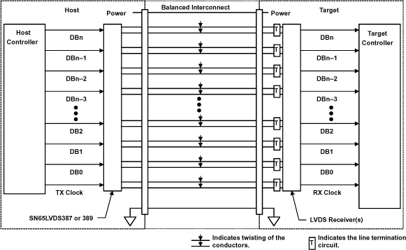
Typical Application Schematic
