SLAS623A November 2008 – November 2016 TAS5342A
PRODUCTION DATA.
- 1 Features
- 2 Applications
- 3 Description
- 4 Revision History
- 5 Pin Configuration and Functions
- 6 Specifications
-
7 Detailed Description
- 7.1 Overview
- 7.2 Functional Block Diagram
- 7.3
Feature Description
- 7.3.1 Mid Z Sequence Compatibility
- 7.3.2 Device Protection System
- 7.3.3 Use Of TAS5342A In High-Modulation-Index Capable Systems
- 7.3.4 Overcurrent (OC) Protection With Current Limiting and Overload Detection
- 7.3.5 Pin-To-Pin Short Circuit Protection System (PPSC)
- 7.3.6 Overtemperature Protection
- 7.3.7 Undervoltage Protection (UVP) and Power-On Reset (POR)
- 7.3.8 Error Reporting
- 7.3.9 Device Reset
- 7.4 Device Functional Modes
- 8 Application and Implementation
- 9 Power Supply Recommendations
- 10Layout
- 11Device and Documentation Support
- 12Mechanical, Packaging, and Orderable Information
Package Options
Mechanical Data (Package|Pins)
- DDV|44
Thermal pad, mechanical data (Package|Pins)
- DDV|44
Orderable Information
8 Application and Implementation
NOTE
Information in the following applications sections is not part of the TI component specification, and TI does not warrant its accuracy or completeness. TI’s customers are responsible for determining suitability of components for their purposes. Customers should validate and test their design implementation to confirm system functionality.
8.1 Application Information
TAS5342A can be configured either in stereo BTL mode, 4 channel SE mode, or mono PBTL mode, depending on output power conditions and system design.
8.2 Typical Applications
8.2.1 Typical Differential (2N) BTL Application
The following schematics and PCB layouts illustrate "best practices" in the use of the TAS5342A.
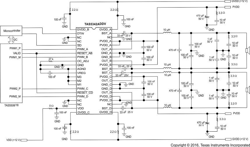 Figure 14. Typical Differential (2N) BTL Application With Ad Modulation Filters
8.2.1.1 Design Requirements
For this design example, use the parameters listed in Table 5 as the input parameters.
Table 5. Design Parameters
| DESIGN PARAMETER | EXAMPLE VALUE |
|---|---|
| Low Power (pull-up) supply | 3.3 V |
| Mid Power Supply (GVDD, VDD) | 12 V |
| High Power Supply (PVDD) | 12 V – 36 V |
| PWM Inputs | INPUT A = 0 – 3.3 V PWM |
| INPUT_B = 0 – 3.3 V PWM | |
| INPUT_C = 0 – 3.3 V PWM | |
| INPUT_D = 0 – 3.3 V PWM | |
| Speaker Impedance | 4 Ω – 8 Ω |
8.2.1.2 Detailed Design Procedure
8.2.1.2.1 PCB Material Recommendation
FR-4 Glass Epoxy material with 2 oz. (70 μm) is recommended for use with the TAS5342A. The use of this material can provide for higher power output, improved thermal performance, and better EMI margin (due to lower PCB trace inductance.
8.2.1.2.2 PVDD Capacitor Recommendation
The large capacitors used in conjunction with each full-birdge, are referred to as the PVDD Capacitors. These capacitors should be selected for proper voltage margin and adequate capacitance to support the power requirements. In practice, with a well designed system power supply, 1000 μF, 50-V supports more applications. The PVDD capacitors should be low ESR type because they are used in a circuit associated with high-speed switching.
8.2.1.2.3 Decoupling Capacitor Recommendations
In order to design an amplifier that has robust performance, passes regulatory requirements, and exhibits good audio performance, good quality decoupling capacitors should be used. In practice, X7R should be used in this application.
The voltage of the decoupling capacitors should be selected in accordance with good design practices. Temperature, ripple current, and voltage overshoot must be considered. This fact is particularly true in the selection of the 0.1 μF that is placed on the power supply to each half-bridge. It must withstand the voltage overshoot of the PWM switching, the heat generated by the amplifier during high power output, and the ripple current created by high-power output. A minimum voltage rating of 50-V is required for use with a 31.5-V power supply.
8.2.1.3 Application Curves
Relevant performance plots for TAS5342A are shown in the BTL Configuration.
Table 6. Performance Plots, Typical BTL Configurations
| PLOT TITLE | FIGURE NUMBER |
|---|---|
| Total Harmonic Distortion + Noise vs. Output power | Figure 1 |
| Output Power vs. Supply Voltage | Figure 2 |
| Unclipped Output Power vs. Supply Voltage | Figure 3 |
| System Efficiency vs. Output Power | Figure 4 |
| System Power Loss vs. Output Power | Figure 5 |
| System Output Power vs. Case Temperature | Figure 6 |
| Noise Amplitude vs. Frequency | Figure 7 |
8.2.2 Typical Non-Differential (1N) BTL
Design Requirements Typical Non-Differential BTL.
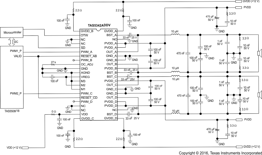 Figure 15. Typical Non-Differential (1N) BTL Application With AD Modulation Filters
8.2.2.1 Design Requirements
For this design example, use the parameters listed in Table 7 as the input parameters.
Table 7. Design Parameters
| DESIGN PARAMETER | EXAMPLE VALUE |
|---|---|
| Low Power (pull-up) supply | 3.3 V |
| Mid Power Supply (GVDD, VDD) | 12 V |
| High Power Supply (PVDD) | 12 V – 36 V |
| PWM Inputs | INPUT A = 0 – 3.3 V PWM |
| INPUT_B = N/C | |
| INPUT_C = 0 – 3.3 V PWM | |
| INPUT_D = N/C | |
| Speaker Impedance | 4 Ω – 8 Ω |
8.2.2.2 Application Curves
Relevant performance plots for TAS5342A are shown in the BTL Configuration.
Table 8. Performance Plots, Typical BTL Configurations
| PLOT TITLE | FIGURE NUMBER |
|---|---|
| Total Harmonic Distortion + Noise vs. Output power | Figure 1 |
| Output Power vs. Supply Voltage | Figure 2 |
| Unclipped Output Power vs. Supply Voltage | Figure 3 |
| System Efficiency vs. Output Power | Figure 4 |
| System Power Loss vs. Output Power | Figure 5 |
| System Output Power vs. Case Temperature | Figure 6 |
| Noise Amplitude vs. Frequency | Figure 7 |
8.2.3 Typical SE Application
Design Requirements Typical SE
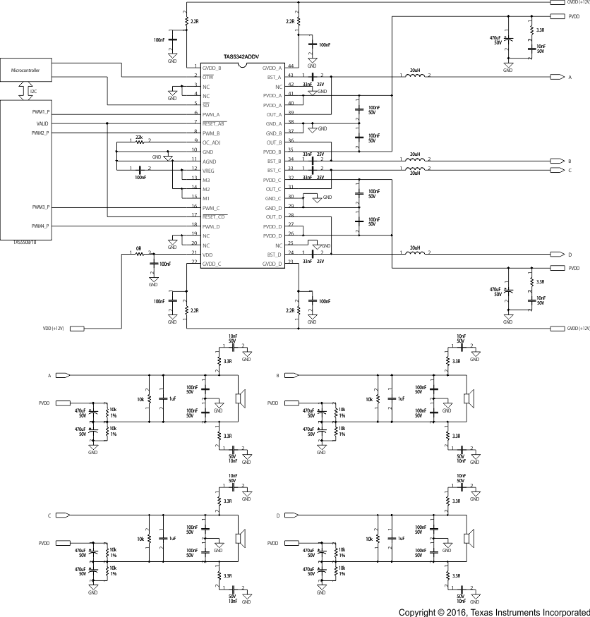 Figure 16. Typical SE Application
8.2.3.1 Design Requirements
For this design example, use the parameters listed in Table 9 as the input parameters.
Table 9. Design Parameters
| DESIGN PARAMETER | EXAMPLE VALUE |
|---|---|
| Low Power (pull-up) supply | 3.3 V |
| Mid Power Supply (GVDD, VDD) | 12 V |
| High Power Supply (PVDD) | 12 V – 36 V |
| PWM Inputs | INPUT A = 0 – 3.3 V PWM |
| NPUT B = 0 – 3.3 V PWM | |
| INPUT_C = 0 – 3.3 V PWM | |
| NPUT D = 0 – 3.3 V PWM | |
| Speaker Impedance | 3 Ω – 4 Ω |
8.2.3.2 Application Curves
Relevant performance plots for TAS5342A are shown in the SE Configuration.
8.2.4 Typical Differential (2N) PBTL Application
Design Requirements Typical Differential PBTL
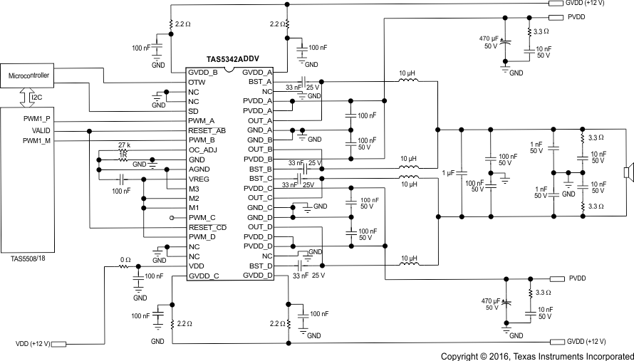 Figure 17. Typical Differential (2N) PBTL Application With AD Modulation Filters
8.2.4.1 Design Requirements
For this design example, use the parameters listed in Table 11 as the input parameters.
Table 11. Design Parameters
| DESIGN PARAMETER | EXAMPLE VALUE |
|---|---|
| Low Power (pull-up) supply | 3.3 V |
| Mid Power Supply (GVDD, VDD) | 12 V |
| High Power Supply (PVDD) | 12 V – 36 V |
| PWM Inputs | INPUT A = 0 – 3.3 V PWM |
| INPUT_B = N/C | |
| INPUT_C = N/C | |
| INPUT_D = GND | |
| Speaker Impedance | 2 Ω – 3 Ω |
8.2.4.2 Application Curves
Relevant performance plots for TAS5342A are shown in the PBTL Configuration.
8.2.5 Typical Non-Differential (1N) PBTL
Design Requirements Typical Non-Differential PBTL.
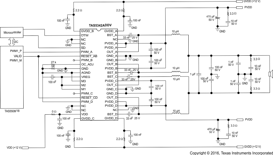 Figure 18. Typical Non-Differential (1N) PBTL Application
8.2.5.1 Design Requirements
For this design example, use the parameters listed in Table 13 as the input parameters.
Table 13. Design Parameters
| DESIGN PARAMETER | EXAMPLE VALUE |
|---|---|
| Low Power (pull-up) supply | 3.3 V |
| Mid Power Supply (GVDD, VDD) | 12 V |
| High Power Supply (PVDD) | 12 V – 36 V |
| PWM Inputs | INPUT A = 0 – 3.3 V PWM |
| INPUT_B = N/C | |
| INPUT_C = N/C | |
| INPUT_D = GND | |
| Speaker Impedance | 2 Ω – 3 Ω |
8.2.5.2 Application Curves
Relevant performance plots for TAS5342A are shown in the PBTL Configuration.
8.3 Systems Examples
A block diagram for a typical audio system using the TAS5342A is shown in Figure 19. The TAS5518 is an
8 channel digital audio PWM processor.
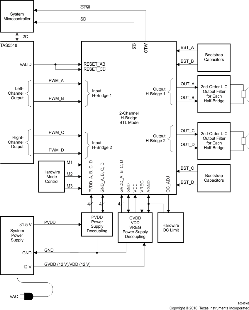 Figure 19. Typical Audio System