SLAS847A May 2012 – March 2015 TAS5612LA
PRODUCTION DATA.
- 1 Features
- 2 Applications
- 3 Description
- 4 Revision History
- 5 Pin Configuration and Functions
- 6 Specifications
-
7 Detailed Description
- 7.1 Overview
- 7.2 Functional Block Diagrams
- 7.3
Feature Description
- 7.3.1 Power Supplies
- 7.3.2 System Power-Up and Power-Down Sequence
- 7.3.3 Start-up and Shutdown Ramp Sequence
- 7.3.4 Unused Output Channels
- 7.3.5 Device Protection System
- 7.3.6 Pin-to-Pin Short-Circuit Protection (PPSC)
- 7.3.7 Overtemperature Protection
- 7.3.8 Overtemperature Warning, OTW
- 7.3.9 Undervoltage Protection (UVP) and Power-On Reset (POR)
- 7.3.10 Error Reporting
- 7.3.11 Fault Handling
- 7.3.12 Device Reset
- 7.3.13 System Design Consideration
- 7.4 Device Functional Modes
- 8 Application and Implementation
- 9 Power Supply Recommendations
- 10Layout
- 11Device and Documentation Support
- 12Mechanical, Packaging, and Orderable Information
Package Options
Mechanical Data (Package|Pins)
- DDV|44
Thermal pad, mechanical data (Package|Pins)
- DDV|44
Orderable Information
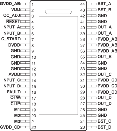
5 Pin Configuration and Functions
DDV Package
44-Pin HTSSOP
Top View

Pin Functions
| PIN | I/O/P(1) | DESCRIPTION | |
|---|---|---|---|
| NAME | NO. | ||
| AVDD | 13 | P | Internal voltage regulator, analog section |
| BST_A | 44 | P | Bootstrap pin, A-side |
| BST_B | 43 | P | Bootstrap pin, B-side |
| BST_C | 24 | P | Bootstrap pin, C-side |
| BST_D | 23 | P | Bootstrap pin, D-side |
| CLIP | 18 | O | Clipping warning, open drain, active low |
| C_START | 7 | O | Start-up ramp |
| DVDD | 8 | P | Internal voltage regulator, digital section |
| FAULT | 16 | O | Shutdown signal, open drain, active low |
| GND | 9, 10, 11, 12, 25, 26, 33, 34, 41, 42 | P | Ground |
| GVDD_AB | 1 | P | Gate-drive voltage supply; AB-side |
| GVDD_CD | 22 | P | Gate-drive voltage supply; CD-side |
| INPUT_A | 5 | I | PWM input signal for half-bridge A |
| INPUT_B | 6 | I | PWM input signal for half-bridge B |
| INPUT_C | 14 | I | PWM input signal for half-bridge C |
| INPUT_D | 15 | I | PWM input signal for half-bridge D |
| M1 | 19 | I | Mode selection 1 (LSB) |
| M2 | 20 | I | Mode selection 2 |
| M3 | 21 | I | Mode selection 3 (MSB) |
| OC_ADJ | 3 | O | Overcurrent threshold programming pin |
| OTW | 17 | O | Overtemperature warning, open drain, active low |
| OUT_A | 39, 40 | O | Output, half-bridge A |
| OUT_B | 35 | O | Output, half-bridge B |
| OUT_C | 32 | O | Output, half-bridge C |
| OUT_D | 27, 28 | O | Output, half-bridge D |
| PVDD_AB | 36, 37, 38 | P | PVDD supply for half-bridge A and B |
| PVDD_CD | 29, 30, 31 | P | PVDD supply for half-bridge C and D |
| RESET | 4 | I | Device reset Input; active low |
| VDD | 2 | P | Input power supply |
| PowerPAD™ | – | P | Ground, connect to grounded heat sink |
(1) I = Input, O = Output, P = Power
Mode Selection Pins
| MODE PINS | PWM Input(1) | OUTPUT CONFIGURATION | INPUT A | INPUT B | INPUT C | INPUT D | MODE | ||
|---|---|---|---|---|---|---|---|---|---|
| M3 | M2 | M1 | |||||||
| 0 | 0 | 0 | 2N + 1 | 2 x BTL | PWMa | PWMb | PWMc | PWMd | AD mode |
| 0 | 0 | 1 | 1N + 1(2) | 2 x BTL | PWMa | Unused | PWMc | Unused | AD mode |
| 0 | 1 | 0 | 2N + 1 | 2 x BTL | PWMa | PWMb | PWMc | PWMd | BD mode |
| 0 | 1 | 1 | 1N + 1(2) | 1 x BTL + 2 x SE | PWMa | Unused | PWMc | PWMd | AD mode |
| 1 | 0 | 0 | 2N + 1 | 1 x PBTL | PWMa | PWMb | 0 | 0 | AD mode |
| 1 | 0 | 0 | 1N + 1(2) | 1 x PBTL | PWMa | Unused | 0 | 1 | AD mode |
| 1 | 0 | 0 | 2N + 1 | 1 x PBTL | PWMa | PWMb | 1 | 0 | BD mode |
| 1 | 0 | 1 | 1N + 1 | 4 x SE(3) | PWMa | PWMb | PWMc | PWMd | AD mode |
(1) The 1N and 2N naming convention is used to indicate the number of PWM lines to the power stage per channel in a specific mode.
(2) Using 1N interface in BTL and PBTL mode results in increased DC offset on the output terminals.
(3) The 4xSE mode can be used as 1xBTL + 2xSE configuration by feeding a 2N PWM signal to either INPUT_AB or INPUT_CD for improved DC offset accuracy