SLOS903B May 2015 – February 2016 TAS5720L , TAS5720M
PRODUCTION DATA.
- 1 Features
- 2 Applications
- 3 Description
- 4 Revision History
- 5 Pin Configuration and Functions
- 6 Specifications
- 7 Detailed Description
- 8 Applications and Implementation
- 9 Power Supply Recommendations
- 10Layout
- 11Device and Documentation Support
- 12Mechanical, Packaging, and Orderable Information
Package Options
Mechanical Data (Package|Pins)
- RSM|32
Thermal pad, mechanical data (Package|Pins)
- RSM|32
Orderable Information
8 Applications and Implementation
NOTE
Information in the following applications sections is not part of the TI component specification, and TI does not warrant its accuracy or completeness. TI’s customers are responsible for determining suitability of components for their purposes. Customers should validate and test their design implementation to confirm system functionality.
8.1 Application Information
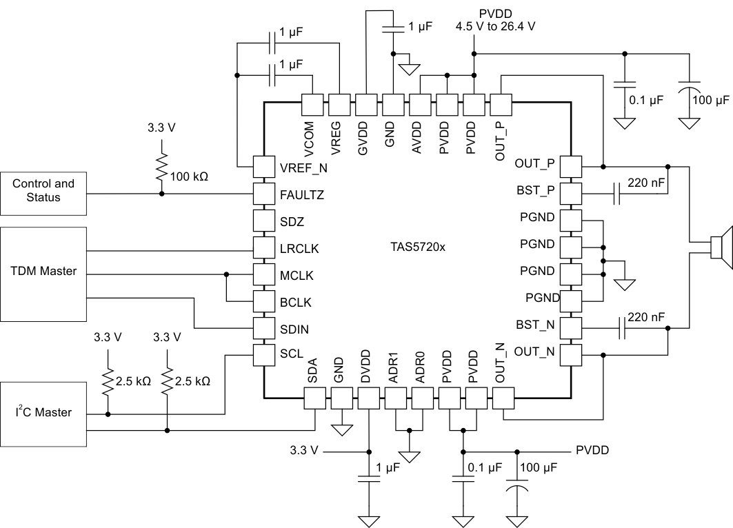
This section describes a filter-free,TDM application.
8.2 Typical Application
 Figure 52. Filter Free 3-Wire TDM Application Circuit (I2C_DEV_ID = 0x6C)
8.2.1 Design Requirements
- Input voltage range PVDD and AVDD: 4.5 V to 26.4 V
- Input voltage range DVDD: 3.3 V to 3.6 V
- Input sample rate: 44.1 kHz to 48 kHz or 88.2 kHz to 96 kHz
- I2C clock frequency: up tp 400 kHz
8.2.2 Design Procedure
8.2.2.1 Overview
The TAS5720L/M is a flexible and easy to use Class D amplifier; therefore the design process is straightforward. Before beginning the design, gather the following information regarding the audio system.
- PVDD rail planned for the design
- Speaker or load impedance
- Audio sample rate
- Maximum output power requirement
- Desired PWM frequency
8.2.2.2 Select the PWM Frequency
Set the PWM frequency by writing to the PWM_RATE bits (bits 6-4, reg 0x06). The default setting for this register is 101, which is 16 × LRCLK for single speed applications and 8 × LRCLK for double speed application. This value equates to a default PWM frequency of 768 kHz for a 48 Hz sample rate.
8.2.2.3 Select the Amplifier Gain and Digital Volume Control
To select the amplifier gain setting, the designer must determine the maximum power target and the speaker impedance. Once the parameters have been determined, calculate the required output voltage swing which delivers the maximum output power.
Choose the lowest analog gain setting that corresponds to produce an output voltage swing greater than the required output swing for maximum power. The analog gain can be set by writing to the ANALOG_GAIN bits (bits 3-2, reg 0x06). The default gain setting is 20.7 dBV referenced to 0dBFS input.
8.2.2.4 Select Input Capacitance
Select the bulk capacitors at the PVDD inputs for proper voltage margin and adequate capacitance to support the power requirements. The TAS5720L/M has very good PVDD PSRR, so the capacitor is more about limiting the ripple and droop for the rest of system than preserving good audio performance. The amount of bulk decoupling can be reduced as long as the droop and ripple is acceptable. One capacitor should be placed near the PVDD inputs at each side of the device. PVDD capacitors should be a low ESR type because they are being used in a high-speed switching application.
8.2.2.5 Select Decoupling Capacitors
Good quality decoupling capacitors should be added at each of the PVDD inputs to provide good reliability, good audio performance, and to meet regulatory requirements. X5R or better ratings should be used in this application. Consider temperature, ripple current, and voltage overshoots when selecting decoupling capacitors. Also, the decoupling capacitors should be located near the PVDD and GND connections to the device to minimize series inductances.
8.2.2.6 Select Bootstrap Capacitors
Each of the outputs require bootstrap capacitors to provide gate drive for the high-side output FETs. For this design, use 0.22-µF, 25-V capacitors of X5R quality or better.
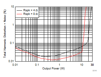
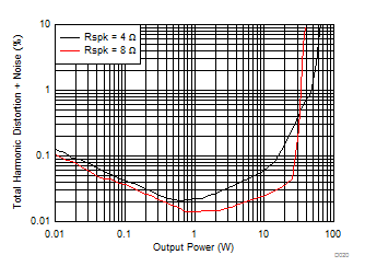
8.2.3 Application Curves

| V(PVDD) = 15 V | f(PWM) = 384 kHz |

| V(PVDD) = 24 V | f(PWM) = 384 kHz |