SCPS274B June 2021 – March 2023 TCA39306
PRODUCTION DATA
- 1 Features
- 2 Applications
- 3 Description
- 4 Revision History
- 5 Pin Configuration and Functions
- 6 Specifications
- 7 Parameter Measurement Information
-
8 Detailed Description
- 8.1
Overview
- 8.1.1 Definition of threshold voltage
- 8.1.2 Correct Device Set Up
- 8.1.3 Disconnecting a Responder from the Main Bus Using the EN Pin
- 8.1.4 Supporting Remote Board Insertion to Backplane with TCA39306
- 8.1.5 Switch Configuration
- 8.1.6 Controller on Side 1 or Side 2 of Device
- 8.1.7 LDO and TCA39306 Concerns
- 8.1.8 Current Limiting Resistance on VREF2
- 8.2 Functional Block Diagram
- 8.3 Feature Description
- 8.4 Device Functional Modes
- 8.1
Overview
- 9 Application and Implementation
- 10Device and Documentation Support
- 11Mechanical, Packaging, and Orderable Information
Package Options
Mechanical Data (Package|Pins)
Thermal pad, mechanical data (Package|Pins)
Orderable Information
3 Description
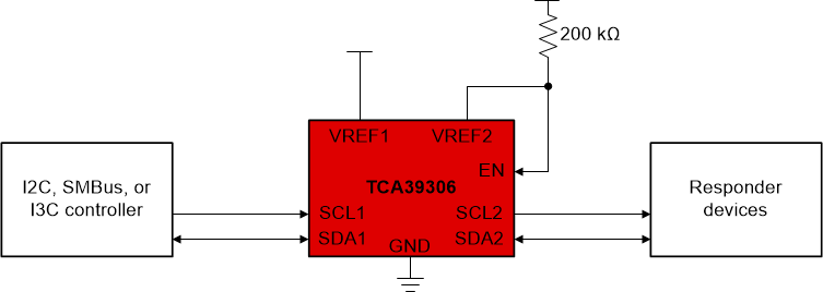
The TCA39306 is a dual bidirectional voltage-level translator compatible with I2C, SMBus, and I3C with an enable (EN) input, and is operational from 0.9-V to 3.3-V VREF1 and 1.8-V to 5.5-V VREF2.
The device allows bidirectional voltage translations between 0.85 V and 5 V, without the use of a direction pin. The low ON-state resistance (RON) of the switch allows connections to be made with minimal propagation delay. When EN is high, the translator switch is ON, and the SCL1 and SDA1 I/O are connected to the SCL2 and SDA2 I/O, respectively, allowing bidirectional data flow between ports. When EN is low, the translator switch is off, and a high-impedance state exists between ports.
In addition to voltage translation, the TCA39306 can be used to isolate a higher speed bus from a lower speed bus by controlling the EN pin to disconnect the slower bus during fast-mode communication.
| PART NUMBER | PACKAGE(1) | BODY SIZE (NOM) |
|---|---|---|
| TCA39306 | VSSOP (8) | 2.30 mm x 2.00 mm |
| SOT-23 (8) | 2.90 mm x 1.60 mm | |
| X2SON (8) | 1.35 mm x 0.80 mm |
 Simplified Application Diagram