SLLSF19 December   2017 TCAN4420

PRODUCTION DATA.  

  1. Features
  2. Applications
  3. Description
    1.     Device Images
      1.      Functional Block Diagram
  4. Revision History
  5. Pin Configuration and Functions
    1.     Pin Functions
  6. Specifications
    1. 6.1 Absolute Maximum Ratings
    2. 6.2 ESD Ratings
    3. 6.3 ESD Ratings Specifications
    4. 6.4 Recommended Operating Conditions
    5. 6.5 Thermal Information
    6. 6.6 Power Supply Characteristics
    7. 6.7 AC and DC Electrical Characteristics
    8. 6.8 Timing Requirements
    9. 6.9 Typical Characteristics
  7. Parameter Measurement Information
  8. Detailed Description
    1. 8.1 Overview
    2. 8.2 Functional Block Diagrams
    3. 8.3 Feature Description
      1. 8.3.1 TXD Dominant Time Out (DTO)
      2. 8.3.2 CAN Bus Short Circuit Current Limiting
      3. 8.3.3 Thermal Shutdown
      4. 8.3.4 Under Voltage Lockout (UVLO) and Unpowered Device
        1. 8.3.4.1 VIO Supply PIN
    4. 8.4 Device Functional Modes
      1. 8.4.1 Polarity Configuration
      2. 8.4.2 Normal Polarity Mode
      3. 8.4.3 Reverse Polarity Mode
      4. 8.4.4 Driver and Receiver Function
      5. 8.4.5 Floating Terminals
  9. Application and Implementation
    1. 9.1 Application Information
    2. 9.2 Typical Application
      1. 9.2.1 Design Requirements
        1. 9.2.1.1 Bus Loading, Length and Number of Nodes
      2. 9.2.2 Detailed Design Procedure
        1. 9.2.2.1 CAN Termination
      3. 9.2.3 Application Curves
  10. 10Power Supply Recommendations
  11. 11Layout
    1. 11.1 Layout Guidelines
    2. 11.2 Layout Example
  12. 12Device and Documentation Support
    1. 12.1 Device Support
      1. 12.1.1 Device Nomenclature
    2. 12.2 Receiving Notification of Documentation Updates
    3. 12.3 Community Resources
    4. 12.4 Trademarks
    5. 12.5 Electrostatic Discharge Caution
    6. 12.6 Glossary
  13. 13Mechanical, Packaging, and Orderable Information

Package Options

Refer to the PDF data sheet for device specific package drawings

Mechanical Data (Package|Pins)
  • D|8
Thermal pad, mechanical data (Package|Pins)
Orderable Information

Pin Configuration and Functions

D Package
8-Pin SOIC
Top View
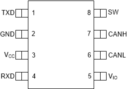
TCAN4420 Pinout_D_TCAN4420.gif

Pin Functions

PINI/ODESCRIPTION
NAMENO.
TXD 1 Logic Input CAN transmit data input (LOW for dominant and HIGH for recessive bus states)
GND 2 Ground Ground connection
VCC 3 Power 5 V ±10% supply voltage
RXD 4 Logic Output CAN receive data output (LOW for dominant and HIGH for recessive bus states)
VIO 5 Power Transceiver I/O level shifting supply voltage
CANL 6 Bus I/O Low level CAN bus input/output line
CANH 7 Bus I/O High level CAN bus input/output line
SW 8 Logic Input Polarity switch pin. Set to low for normal polarity (default), and high to reverse the polarity of the CAN pins