SNAS686 May 2016 TDC7201
PRODUCTION DATA.
- 1 Features
- 2 Applications
- 3 Description
- 4 Revision History
- 5 Pin Configuration and Functions
- 6 Specifications
-
7 Detailed Description
- 7.1 Overview
- 7.2 Functional Block Diagram
- 7.3 Feature Description
- 7.4 Device Functional Modes
- 7.5 Programming
- 7.6
Register Maps
- 7.6.1 Register Initialization
- 7.6.2 TDCx_CONFIG1: TDCx Configuration Register 1 R/W (address = 00h, CSBx asserted) [reset = 0h]
- 7.6.3 TDCx_CONFIG2: TDCx Configuration Register 2 R/W (address = 01h, CSBx asserted) [reset = 40h]
- 7.6.4 TDCx_INT_STATUS: Interrupt Status Register (address = 02h, CSBx asserted) [reset = 00h]
- 7.6.5 TDCx_INT_MASK: TDCx Interrupt Mask Register R/W (address = 03h, CSBx asserted) [reset = 07h]
- 7.6.6 TDCx_COARSE_CNTR_OVF_H: Coarse Counter Overflow High Value Register (address = 04h, CSBx asserted) [reset = FFh]
- 7.6.7 TDCx_COARSE_CNTR_OVF_L: TDCx Coarse Counter Overflow Low Value Register (address = 05h, CSBx asserted) [reset = FFh ]
- 7.6.8 TDCx_CLOCK_CNTR_OVF_H: Clock Counter Overflow High Register (address = 06h, CSBx asserted) [reset = FFh]
- 7.6.9 TDCx_CLOCK_CNTR_OVF_L: Clock Counter Overflow Low Register (address = 07h, CSBx asserted) [reset = FFh]
- 7.6.10 TDCx_CLOCK_CNTR_STOP_MASK_H: CLOCK Counter STOP Mask High Value Register (address = 08h, CSBx asserted) [reset = 00h]
- 7.6.11 TDCx_CLOCK_CNTR_STOP_MASK_L: CLOCK Counter STOP Mask Low Value Register (address = 09h, CSBx asserted) [reset = 00h]
- 7.6.12 TDCx_TIME1: Time 1 Register (address: 10h, CSBx asserted) [reset = 00_0000h]
- 7.6.13 TDCx_CLOCK_COUNT1: Clock Count Register (address: 11h, CSBx asserted) [reset = 00_0000h]
- 7.6.14 TDCx_TIME2: Time 2 Register (address: 12h, CSBx asserted) [reset = 00_0000h]
- 7.6.15 TDCx_CLOCK_COUNT2: Clock Count Register (address: 13h, CSBx asserted) [reset = 00_0000h]
- 7.6.16 TDCx_TIME3: Time 3 Register (address: 14h, CSBx asserted) [reset = 00_0000h]
- 7.6.17 TDCx_CLOCK_COUNT3: Clock Count Registers (address: 15h, CSBx asserted) [reset = 00_0000h]
- 7.6.18 TDCx_TIME4: Time 4 Register (address: 16h, CSBx asserted) [reset = 00_0000h]
- 7.6.19 TDCx_CLOCK_COUNT4: Clock Count Register (address: 17h, CSBx asserted) [reset = 00_0000h]
- 7.6.20 TDCx_TIME5: Time 5 Register (address: 18h, CSBx asserted) [reset = 00_0000h]
- 7.6.21 TDCx_CLOCK_COUNT5: Clock Count Register (address: 19h, CSBx asserted) [reset = 00_0000h]
- 7.6.22 TDCx_TIME6: Time 6 Register (address: 1Ah, CSBx asserted) [reset = 00_0000h]
- 7.6.23 TDCx_CALIBRATION1: Calibration 1 Register (address: 1Bh, CSBx asserted) [reset = 00_0000h]
- 7.6.24 TDCx_CALIBRATION2: Calibration 2 Register (address: 1Ch, CSBx asserted) [reset = 00_0000h]
- 8 Application and Implementation
- 9 Power Supply Recommendations
- 10Layout
- 11Device and Documentation Support
- 12Mechanical, Packaging, and Orderable Information
Package Options
Mechanical Data (Package|Pins)
- ZAX|25
Thermal pad, mechanical data (Package|Pins)
Orderable Information
8 Application and Implementation
NOTE
Information in the following applications sections is not part of the TI component specification, and TI does not warrant its accuracy or completeness. TI’s customers are responsible for determining suitability of components for their purposes. Customers should validate and test their design implementation to confirm system functionality.
8.1 Application Information
The TDC7201 is targeted for the TOF measurement of laser pulses. Laser based time-of-flight applications demand picosecond accuracy plus the ability to measure very short durations. The TDC7201 is highly suited for such applications with its wide measurement range of 0.25 ns to 8 ms and high accuracy of 28 ps. It has a single shot resolution of 55 ps which is equivalent to 0.825 cm.
8.2 Typical Application
The TDC7201 can be used in TOF laser range finders to measure distance to a target. Besides surveying and navigation, distance measurement using TOF laser range finders is used for collision avoidance and safety in a number of systems like drones, robotics, and autonomous vehicles. A block diagram of TOF laser range finders is shown in Figure 50. The system consists of a laser pulse emitter or transmitter, an echo receiver, and a TDC. In this system, TDC7201 can measure the round trip time between a light pulse emission and its echo from the target. The light pulse transmitter triggers the TDC7201 measurement by providing the start input and the receiver stops the TDC7201. Using the equation D = C × TOF / 2, where C is the speed of light, the distance D to the target can be calculated once the TOF is known. A TOF of 0.67 ns is equivalent to 10 cm range and 1 cm accuracy corresponds to 67 ps.
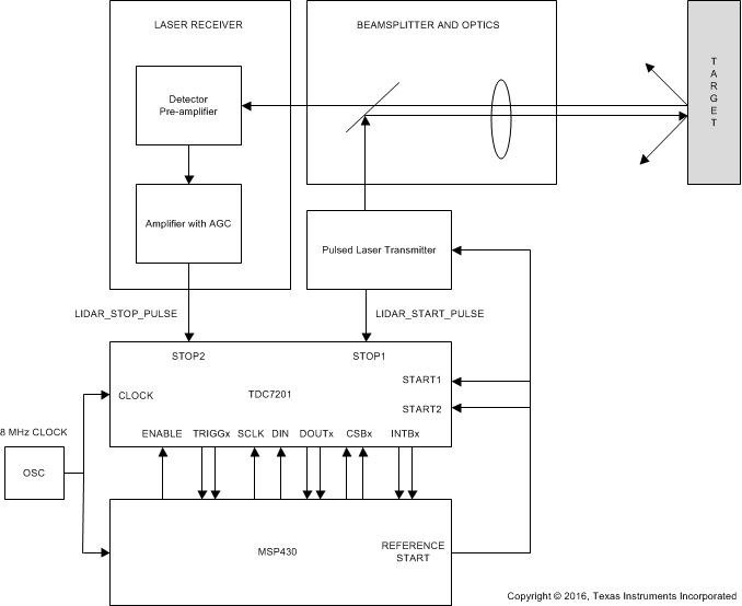 Figure 50. TDC7201 Based TOF Laser Range Finder Block Diagram
8.2.1 Design Requirements
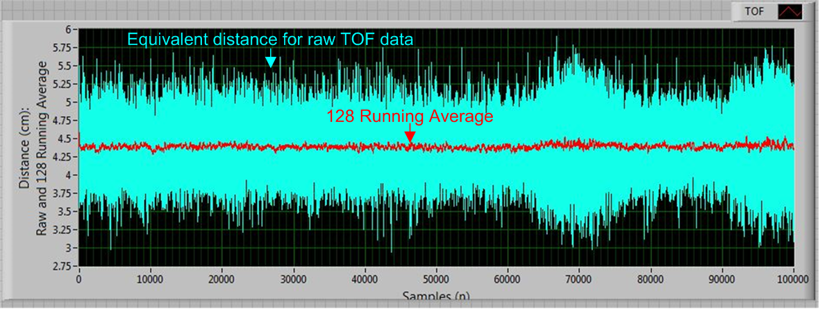
The TOF measurement design is driven by the extreme low measurement range and high accuracy constraints. The TDC7201 has two built-in TDCs to achieve a low measurement range of 4 cm (equivalent to a 0.25 ns TOF). The TDC7201 with its single shot resolution of 55 ps (which is equivalent to 0.825 cm) and built-in averaging of up to 128 samples can enable applications to achieve millimeter or even sub-millimeter precision.
8.2.2 Detailed Design Procedure
8.2.2.1 Measuring Time Periods Less Than 12 ns Using TDC7201
The minimum time measurable in measurement mode 1 is 12 ns. It is feasible to do measurements down to 0.25 ns using the TDC7201 in what is called combined measurement mode. In combined measurement mode, START1 and START2 are connected together:
- A common REFERENCE_START signal is applied to START1 and START2 at least 12 ns before occurrence of actual Start and Stop signals
- TOF Start (LIDAR_START) signal is connected to STOP1
- TOF Stop signal (LIDAR_STOP) is connected to STOP2
- Two time periods T1 (REFERENCE_START to LIDAR_START) and T2 (REFERENCE_START to LIDAR_STOP) are measured and their difference T3 = (T2 - T1) is the required TOF
An illustration of this combined measurement mode is shown in Figure 51 and Figure 52. It is necessary that the REFERENCE_START pulse is generated at least 12 ns before the LIDAR_START pulse. The REFERENCE_START could be generated by the MCU or by some other timing circuit.
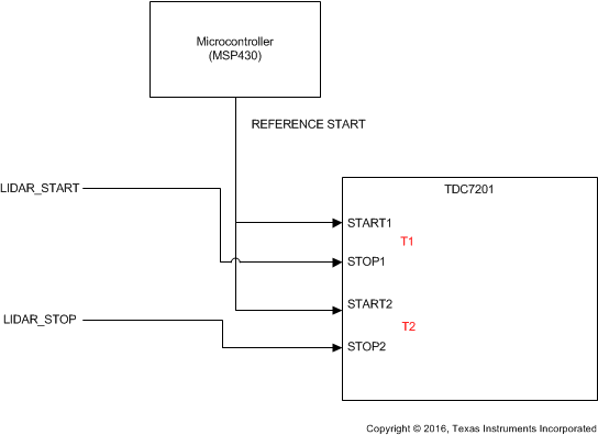 Figure 51. Short Time Measurement Setup
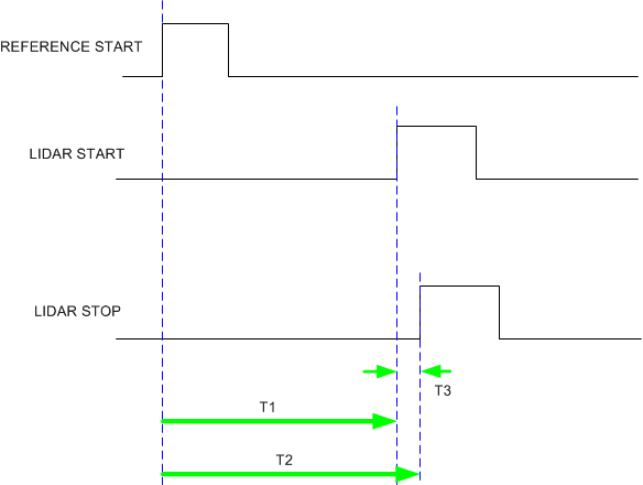 Figure 52. TDC7201 Short Time Measurement Timing
8.2.3 Application Curves
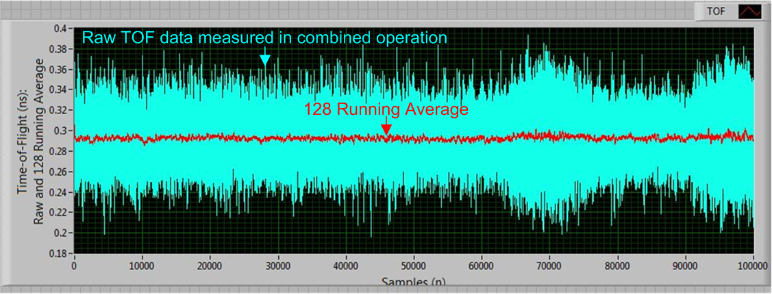
Figure 53 and Figure 54 show a TOF measurement of 0.25ns using the TDC7201 in combined measurement mode. A Tektronix DTG5078 based test setup was used to generate the TDC7201 START, STOP inputs.
8.3 CLOCK Recommendations
A stable, known reference clock is crucial to the ability to measure time, regardless of the time measuring device. Two parameters of a clock source primarily affect the ability to measure time: accuracy and jitter. The following subsection will discuss recommendations for the CLOCK in order to increase accuracy and reduce jitter.
8.3.1 CLOCK Accuracy
CLOCK sources are typically specified with an accuracy value as the clock period is not exactly equal to the nominal value specified. For example, an 8-MHz clock reference may have a 20-ppm accuracy. The true value of the clock period therefore has an error of ±20 ppm, and the real frequency is in the range 7.99984 MHz to 8.00016 MHz [8 MHz ± (8 MHz) x (20/106)].
If the clock accuracy is at this boundary, but the reference time used to calculate the time of flight relates to the nominal 8-MHz clock period, then the time measured will be affected by this error. For example, if the time period measured is 50 µs, and the 8-MHz reference clock has +50 ppm of error in frequency, but the time measured refers to the 125-ns period (1/8 MHz), then the 50 µs time period will have an error of 50 µs x 50/1000000 = 2.5 ns.
In summary, a clock inaccuracy translates proportionally to a time measurement error.
8.3.2 CLOCK Jitter
Clock jitter introduces uncertainty into a time measurement, rather than inaccuracy. As shown in Figure 55, the jitter accumulates on each clock cycle so the uncertainty associated to a time measurement is a function of the clock jitter and the number of clock cycles measured.
Clock_Jitter_Uncertainty = (√n) × (θJITTER), where n is the number of clock cycles counted, and θJITTER is the cycle-to-cycle jitter of the clock.
For example, if the time measured is 50 μs using an 8-MHz reference clock, n = 50 μs/(1/8 MHz) = 400 clock cycles. If the RMS cycle-to-cycle jitter, θJITTER = 10 ps, then the RMS uncertainty introduced in a single measurement is in the order of (√n) × (θJITTER) = 200 ps.
Because the effect of jitter is random, averaging or accumulating time results reduces the effect of the uncertainty introduced. If the time is measured m times and the result is averaged, then the uncertainty is reduced to: Clock_Jitter_Uncertainty = (√n) × (θJITTER) / (√m).
For example, if 64 averages are performed in the example above, then the jitter-related uncertainty is reduced to 25 ps RMS.
 Figure 55. CLOCK Jitter