SLOS547A November   2008  – November 2015 THS4509-Q1

PRODUCTION DATA.  

  1. Features
  2. Applications
  3. Description
  4. Revision History
  5. Pin Configuration and Functions
  6. Specifications
    1. 6.1 Absolute Maximum Ratings
    2. 6.2 ESD Ratings
    3. 6.3 Recommended Operating Conditions
    4. 6.4 Thermal Information
    5. 6.5 Electrical Characteristics: VS+ - VS- = 5 V
    6. 6.6 Electrical Characteristics: VS+ - VS- = 3 V
    7. 6.7 Typical Characteristics
      1. 6.7.1 Typical Characteristics: VS+ - VS- = 5 V
      2. 6.7.2 Typical Characteristics: VS+ - VS- = 3 V
  7. Detailed Description
    1. 7.1 Overview
    2. 7.2 Functional Block Diagram
    3. 7.3 Feature Description
    4. 7.4 Device Functional Modes
  8. Application and Implementation
    1. 8.1 Application Information
      1. 8.1.1 Test Circuits
        1. 8.1.1.1 Frequency Response
        2. 8.1.1.2 Distortion and 1-dB Compression
        3. 8.1.1.3 S-Parameter, Slew Rate, Transient Response, Settling Time, Output Impedance, Overdrive, Output Voltage, and Turn-On and Turn-Off Time
        4. 8.1.1.4 CM Input
        5. 8.1.1.5 CMRR and PSRR
      2. 8.1.2 Differential Input to Differential Output Amplifier
      3. 8.1.3 Single-Ended Input to Differential Output Amplifier
      4. 8.1.4 Input Common-Mode Voltage Range
      5. 8.1.5 Setting the Output Common-Mode Voltage
      6. 8.1.6 Single-Supply Operation (3 V to 5 V)
    2. 8.2 Typical Applications
      1. 8.2.1 THS4509-Q1 + ADS5500-EP Combined Performance
        1. 8.2.1.1 Design Requirements
        2. 8.2.1.2 Detailed Design Procedure
        3. 8.2.1.3 Application Curves
      2. 8.2.2 THS4509-Q1 + ADS5424-SP Combined Performance
        1. 8.2.2.1 Detailed Design Procedure
        2. 8.2.2.2 Application Curve
  9. Power Supply Recommendations
  10. 10Layout
    1. 10.1 Layout Guidelines
      1. 10.1.1 THS4509-Q1 EVM
      2. 10.1.2 EVM Warnings and Restrictions
    2. 10.2 Layout Example
  11. 11Device and Documentation Support
    1. 11.1 Documentation Support
      1. 11.1.1 Related Documentation
    2. 11.2 Community Resources
    3. 11.3 Trademarks
    4. 11.4 Electrostatic Discharge Caution
    5. 11.5 Glossary
  12. 12Mechanical, Packaging, and Orderable Information

Package Options

Mechanical Data (Package|Pins)
Thermal pad, mechanical data (Package|Pins)
Orderable Information

9 Power Supply Recommendations

The THS4509-Q1 can be used with any combination of positive and negative power supplies as long as the combined supply voltage is between 3 V and 5 V. The THS4509-Q1 will provide best performance when the output voltage is set at the mid supply voltage, and when the total supply voltage is between 3 V and 5 V. Power supply bypassing as shown in Figure 93 and Figure 92 is important and power supply regulation should be within 5% or better when using a supply voltage near the edges of the operating range.
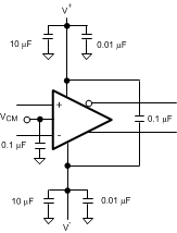
THS4509-Q1 20130101.gif Figure 92. Split Supply Bypassing Capacitors
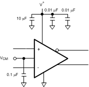
THS4509-Q1 20130112.gif Figure 93. Single Supply Bypassing Capacitors