SLOS829A February 2013 – July 2015 THS4532
PRODUCTION DATA.
- 1 Features
- 2 Applications
- 3 Description
- 4 Revision History
- 5 Related Products
- 6 Pin Configuration and Functions
- 7 Specifications
- 8 Detailed Description
-
9 Application and Implementation
- 9.1
Application Information
- 9.1.1 Frequency Response and Output Impedance
- 9.1.2 Distortion
- 9.1.3 Slew Rate, Transient Response, Settling Time, Overdrive, Output Voltage, and Turnon and Turnoff Time
- 9.1.4 Common-Mode and Power Supply Rejection
- 9.1.5 VOCM Input
- 9.1.6 Balance Error
- 9.1.7 Single-Supply Operation
- 9.1.8 Low-Power Applications and the Effects of Resistor Values on Bandwidth
- 9.1.9 Driving Capacitive Loads
- 9.1.10 Audio Performance
- 9.1.11 Audio On and Off Pop Performance
- 9.2 Typical Applications
- 9.3 Systems Examples
- 9.1
Application Information
- 10Power Supply Recommendations
- 11Layout
- 12Device and Documentation Support
- 13Mechanical, Packaging, and Orderable Information
Package Options
Mechanical Data (Package|Pins)
- PW|16
Thermal pad, mechanical data (Package|Pins)
Orderable Information
11 Layout
11.1 Layout Guidelines
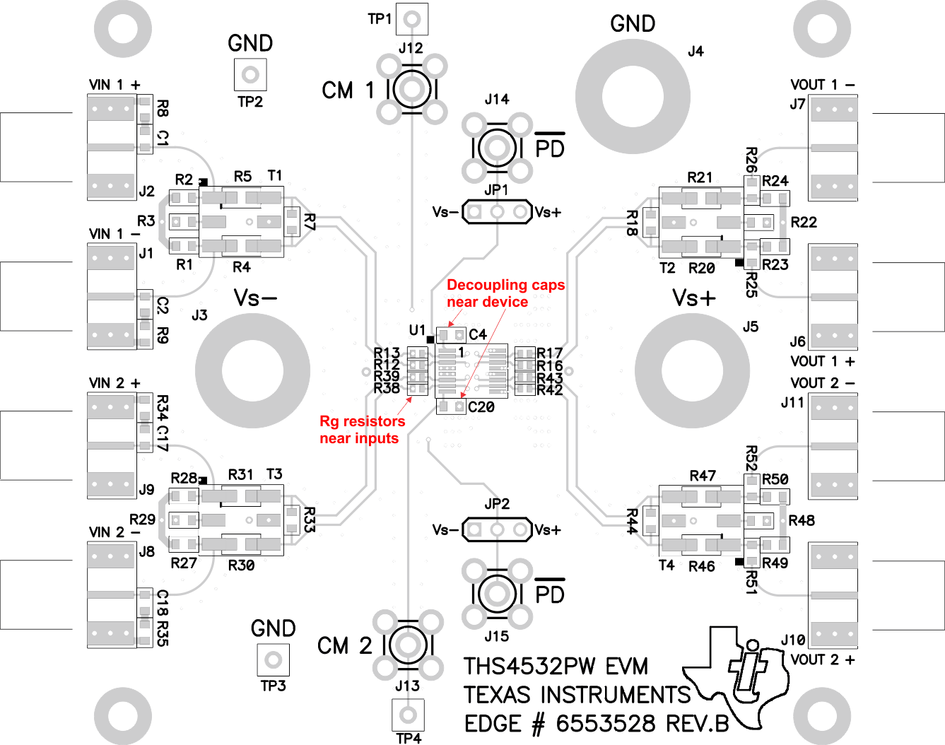
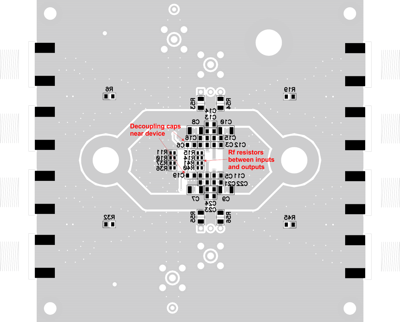
The THS4532 EVM (SLOU356) should be used as a reference when designing the circuit board. TI recommends following the EVM layout of the external components near to the amplifier, ground plane construction, and power routing as closely as possible. General guidelines are:
- Signal routing should be direct and as short as possible into and out of the amplifier.
- The feedback path should be short and direct avoiding vias if possible.
- Ground or power planes should be removed from directly under the amplifier’s input and output pins.
- A series output resistor is recommended to be placed as near to the output pin as possible. See Figure 79 for recommended values given expected capacitive load of design.
- A 2.2-µF power supply decoupling capacitor should be placed within 2 inches of the device and can be shared with other amplifiers. For split supply, a capacitor is required for both supplies.
- A 0.1-µF power supply decoupling capacitor should be placed as near to the power supply pins as possible. Preferably within 0.1 inch. For split supply, a capacitor is required for both supplies.
- The PD pin uses TTL logic levels referenced to the negative supply voltage (VS-). When not used it should tied to the positive supply to enable the amplifier. When used, it must be actively driven high or low and should not be left in an indeterminate logic state. A bypass capacitor is not required, but can be used for robustness in noisy environments.
11.2 Layout Example
Figure 100 through Figure 103 illustrate the PCB layers of the EVM.
 Figure 100. THS4532 EVM Top Layer 1
 Figure 101. THS4532 EVM Ground Layer 2
 Figure 102. THS4532 EVM Ground Layer 3
 Figure 103. THS4532 EVM Bottom Layer 4