SBOS431A May 2009 – March 2017 THS6214
PRODUCTION DATA.
- 1 Features
- 2 Applications
- 3 Description
- 4 Revision History
- 5 Pin Configuration and Functions
-
6 Specifications
- 6.1 Absolute Maximum Ratings
- 6.2 ESD Ratings
- 6.3 Recommended Operating Conditions
- 6.4 Thermal Information
- 6.5 Electrical Characteristics: VS = ±12 V
- 6.6 Electrical Characteristics: VS = ±6 V
- 6.7 Timing Requirements
- 6.8 Typical Characteristics: VS = ±12 V, Full Bias
- 6.9 Typical Characteristics: VS = ±12 V, Mid Bias
- 6.10 Typical Characteristics: VS = ±12 V, Low Bias
- 6.11 Typical Characteristics: VS = ±6 V, Full Bias
- 6.12 Typical Characteristics: VS = ±6 V, Mid Bias
- 6.13 Typical Characteristics: VS = ±6 V, Low Bias
- 7 Detailed Description
- 8 Application and Implementation
- 9 Power Supply Recommendations
- 10Layout
- 11Device and Documentation Support
- 12Mechanical, Packaging, and Orderable Information
Package Options
Mechanical Data (Package|Pins)
Thermal pad, mechanical data (Package|Pins)
- PWP|24
Orderable Information
1 Features
- Low Power Consumption:
- Full Bias Mode: 21 mA per Port
- Mid Bias Mode: 16.2 mA per Port
- Low Bias Mode: 11.2 mA per Port
- Low-Power Shutdown Mode
- IADJ Pin for Variable Bias
- Low Noise:
- Voltage Noise: 2.7 nV/√Hz
- Inverting Current Noise: 17 pA/√Hz
- Noninverting Current Noise: 1.2 pA/√Hz
- Low MTPR Distortion:
- 70 dB with 20.5 dBm G.993.2—Profile 8b
- –93 dBc HD3 (1 MHz, 100-Ω Differential)
- High Output Current: > 416 mA (25-Ω Load)
- Wide Output Swing: 43.2 VPP (±12 V, 100-Ω Differential Load)
- Wide Bandwidth: 150 MHz (GDIFF = 10 V/V)
- PSRR: 50 dB at 1 MHz for Good Isolation
- Wide Power-Supply Range: 10 V to 28 V
2 Applications
3 Description
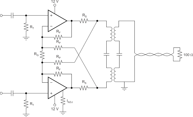
The THS6214 is a dual-port, current-feedback architecture, differential line driver amplifier system ideal for xDSL systems. The device is targeted for use in very-high-bit-rate digital subscriber line 2 (VDSL2) line driver systems that enable greater than 14.5-dBm line power, supporting the G.993.2 VDSL2 17a profile. The device is also fast enough to support central-office transmissions of 14.5-dBm line power up to 30 MHz. The device is also targeted for use as a broadband or wideband power line communications (PLC) amplifier for line driver applications.
The unique architecture of the THS6214 uses minimal quiescent current and still achieves very high linearity. Differential distortion, under full bias conditions, is –93 dBc at 1 MHz and reduces to only –73 dBc at 10 MHz. Fixed multiple bias settings of the amplifiers allow for enhanced power savings for line lengths where the full performance of the amplifier is not required. To allow for even more flexibility and power savings, an adjustable current pin (IADJ) is available to further lower the bias currents.
The wide output swing of 43.2 VPP (100-Ω differential load) with ±12-V power supplies, coupled with over 416-mA current drive (25-Ω load), allows for wide dynamic headroom, keeping distortion minimal.
The THS6214 is available in a VQFN-24 or a HTSSOP-24 PowerPAD™ package.
Device Information(1)
| PART NUMBER | PACKAGE | BODY SIZE (NOM) |
|---|---|---|
| THS6214 | VQFN (24) | 5.00 mm × 4.00 mm |
| HTSSOP (24) | 7.80 mm × 4.40 mm |
- For all available packages, see the orderable addendum at the end of the data sheet.
Typical VDSL2 Line Driver Circuit Using One Port of the THS6214
