SBOS431A May 2009 – March 2017 THS6214
PRODUCTION DATA.
- 1 Features
- 2 Applications
- 3 Description
- 4 Revision History
- 5 Pin Configuration and Functions
-
6 Specifications
- 6.1 Absolute Maximum Ratings
- 6.2 ESD Ratings
- 6.3 Recommended Operating Conditions
- 6.4 Thermal Information
- 6.5 Electrical Characteristics: VS = ±12 V
- 6.6 Electrical Characteristics: VS = ±6 V
- 6.7 Timing Requirements
- 6.8 Typical Characteristics: VS = ±12 V, Full Bias
- 6.9 Typical Characteristics: VS = ±12 V, Mid Bias
- 6.10 Typical Characteristics: VS = ±12 V, Low Bias
- 6.11 Typical Characteristics: VS = ±6 V, Full Bias
- 6.12 Typical Characteristics: VS = ±6 V, Mid Bias
- 6.13 Typical Characteristics: VS = ±6 V, Low Bias
- 7 Detailed Description
- 8 Application and Implementation
- 9 Power Supply Recommendations
- 10Layout
- 11Device and Documentation Support
- 12Mechanical, Packaging, and Orderable Information
Package Options
Mechanical Data (Package|Pins)
Thermal pad, mechanical data (Package|Pins)
- PWP|24
Orderable Information
8 Application and Implementation
NOTE
Information in the following applications sections is not part of the TI component specification, and TI does not warrant its accuracy or completeness. TI’s customers are responsible for determining suitability of components for their purposes. Customers should validate and test their design implementation to confirm system functionality.
8.1 Application Information
The THS6214 is typically used to drive high output power applications with various load conditions. In the Typical Applications section, the amplifier is presented in a general-purpose, wideband, current-feedback configuration, and a more specific 100-Ω twisted pair cable line driver. However, the amplifier is also applicable for many different general-purpose and specific cable line-driving scenarios beyond what is described in the Typical Applications section.
8.2 Typical Applications
8.2.1 Wideband Current-Feedback Operation
The THS6214 provides the exceptional ac performance of a wideband current-feedback op amp with a highly linear, high-power output stage. Requiring only 21-mA/port quiescent current, the THS6214 swings to within 1.9 V of either supply rail on a 100-Ω load and delivers in excess of 416 mA at room temperature. This low-output headroom requirement, along with supply voltage independent biasing, provides remarkable ±6-V supply operation. The THS6214 delivers greater than 140-MHz bandwidth driving a 2-VPP output into 100 Ω on a ±6-V supply. Previous boosted output stage amplifiers typically suffer from very poor crossover distortion when the output current goes through zero. The THS6214 achieves a comparable power gain with much better linearity. The primary advantage of a current-feedback op amp over a voltage-feedback op amp is that ac performance (bandwidth and distortion) is relatively independent of signal gain. Figure 81 shows the dc-coupled, gain of 10 V/V, dual power-supply circuit configuration used as the basis of the ±12-V Electrical Characteristics and Typical Characteristics. For test purposes, the input impedance is set to 50 Ω with a resistor to ground and the output impedance is set to 50 Ω with a series output resistor. Voltage swings reported in the Electrical Characteristics are taken directly at the input and output pins, whereas load powers (dBm) are defined at a matched 50-Ω load.
For the circuit of Figure 81, the total effective load is 100 Ω || 1.24 kΩ || 1.24 kΩ = 86.1 Ω.
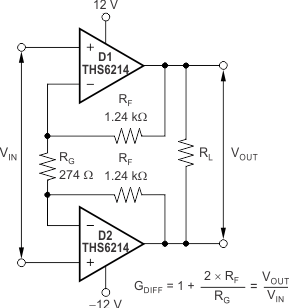 Figure 81. Noninverting Differential I/O Amplifier
8.2.1.1 Design Requirements
The main design requirements for wideband current-feedback operation are to choose power supplies that satisfy common-mode requirements at the input and output of the device, and also to use a feedback resistor value that allows for the proper bandwidth when maintaining stability. These requirements and the proper solutions are described in the Detailed Design Procedure section. Using transformers and split power supplies can be required for certain applications.
8.2.1.2 Detailed Design Procedure
For ease of test purposes in this design, the THS6214 input impedance is set to 50 Ω with a resistor to ground and the output impedance is set to 50 Ω with a series output resistor. Voltage swings reported in the Electrical Characteristics tables are taken directly at the input and output pins, whereas load powers (dBm) are defined at a matched 50-Ω load. For the circuit of Figure 81, the total effective load is 100 Ω || 1.24 kΩ || 1.24 kΩ = 86.1 Ω. This approach allows a source termination impedance to be set at the input that is independent of the signal gain. For instance, simple differential filters can be included in the signal path right up to the noninverting inputs with no interaction with the gain setting. The differential signal gain for the circuit of Figure 81 is given by Equation 5:

where
- AD = differential gain
A value of 274 Ω for the AD = 10-V/V design is given by Figure 81. The device bandwidth is primarily controlled with the feedback resistor value because the THS6214 is a current-feedback (CFB) amplifier; the differential gain, however, can be adjusted with considerable freedom using just the RG resistor. In fact, RG can be reduced by a reactive network that provides a very isolated shaping to the differential frequency response.
Various combinations of single-supply or ac-coupled gain can also be delivered using the basic circuit of Figure 81. Common-mode bias voltages on the two noninverting inputs pass on to the output with a gain of 1 V/V because an equal dc voltage at each inverting node does not create current through RG. This circuit does show a common-mode gain of 1 V/V from the input to output. The source connection must either remove this common-mode signal if undesired (using an input transformer can provide this function), or the common-mode voltage at the inputs can be used to set the output common-mode bias. If the low common-mode rejection of this circuit is a problem, the output interface can also be used to reject that common-mode signal. For instance, most modern differential input analog-to-digital converters (ADCs) reject common-mode signals very well, and a line-driver application through a transformer also attenuates the common-mode signal through to the line.
8.2.1.3 Application Curves
Figure 82 and Figure 83 show the frequency response and distortion performance of the circuit in Figure 81. The measurements are made with a load resistor (RL) of 100 Ω, and at room temperature. Figure 82 is measured using the three different device power modes, and the distortion measurements in Figure 83 are made at an output voltage level of 2 VPP.
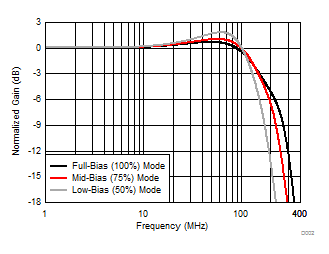 Figure 82. Frequency Response
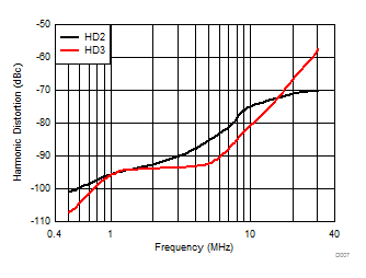 Figure 83. Harmonic Distortion
8.2.2 Dual-Supply VDSL Downstream Driver
Figure 84 shows an example of a dual-supply downstream driver with a synthesized output impedance circuit. The THS6214 is configured as a differential gain stage to provide a signal drive to the primary winding of the transformer (a step-up transformer with a turns ratio of 1:n is shown in Figure 84). The main advantage of this configuration is the cancellation of all even harmonic-distortion products. Another important advantage is that each amplifier must only swing half of the total output required driving the load.
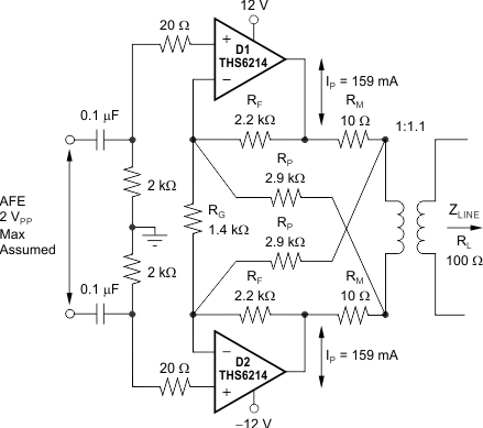 Figure 84. Dual-Supply VDSL Downstream Driver
The analog front-end (AFE) signal is ac-coupled to the driver, and the noninverting input of each amplifier is biased to the mid-supply voltage (ground in this case). In addition to providing the proper biasing to the amplifier, this approach also provides a high-pass filtering with a corner frequency that is set at 5 kHz in this example. Because the signal bandwidth starts at 26 kHz, this high-pass filter does not generate any problems and has the advantage of filtering out unwanted lower frequencies.
8.2.2.1 Design Requirements
The main design requirements for Figure 84 are to match the output impedance correctly, satisfy headroom requirements, and ensure that the circuit meets power driving requirements. These requirements are described in the Detailed Design Procedure section and include the required equations to properly implement the design. The design must be fully worked through before physical implementation because small changes in a single parameter can often have large effects on performance.
8.2.2.2 Detailed Design Procedure
For Figure 84, the input signal is amplified with a gain set by Equation 6:

The two back-termination resistors (RM = 10 Ω, each) added at each terminal of the transformer make the impedance of the amplifier match the impedance of the line, and also provide a means of detecting the received signal for the receiver. The value of these resistors (RM) is a function of the line impedance and the transformer turns ratio (n), given by Equation 7:

8.2.2.2.1 Line Driver Headroom Model Requirements
The first step in a transformer-coupled, twisted-pair driver design is to compute the peak-to-peak output voltage from the target specifications. This calculation is done using Equation 8 to Equation 11:

where
- PL = power at the load
- VRMS = voltage at the load
- RL = load impedance
These values produce the following:


where
- VP = peak voltage at the load
- CF = crest factor

where
- VLPP = peak-to-peak voltage at the load
Consolidating Equation 8 to Equation 11 allows the required peak-to-peak voltage at the load to be expressed as a function of the crest factor, the load impedance, and the power at the load, as given by Equation 12:

VLPP is usually computed for a nominal line impedance and can be taken as a fixed design target.
The next step in the design is to compute the individual amplifier output voltage and currents as a function of peak-to-peak voltage on the line and transformer-turns ratio.
When this turns ratio changes, the minimum allowed supply voltage also changes. The peak current in the amplifier output is given by Equation 13:

where
- VPP is as defined in Equation 12, and
- RM is as defined in Equation 7 and Figure 85
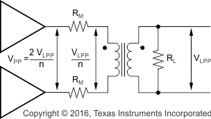 Figure 85. Driver Peak Output Voltage
With the previous information available, a supply voltage and the turns ratio desired for the transformer can now be selected, and the headroom for the THS6214 can be calculated.
The model illustrated in Figure 86 can be described with Equation 14 and Equation 15 as:
- The available output swing:
- Or as the required supply voltage:


The minimum supply voltage for power and load requirements is given by Equation 15.
V1, V2, R1, and R2 are given in Table 3 for the ±12-V operation.
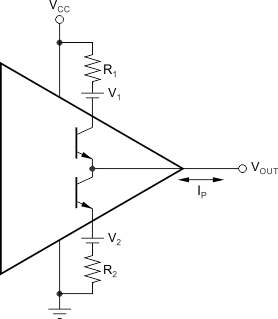 Figure 86. Line Driver Headroom Model
Table 3. Line Driver Headroom Model Values
| VS | V1 | R1 | V2 | R2 |
|---|---|---|---|---|
| ±12 V | 1 V | 0.6 Ω | 1 V | 1.2 Ω |
When using a synthetic output impedance circuit (see Figure 84), a significant drop in bandwidth occurs from the specification provided in the Electrical Characteristics tables. This apparent drop in bandwidth for the differential signal is a result of the apparent increase in the feedback transimpedance for each amplifier. This feedback transimpedance equation is given by Equation 16:

To increase the 0.1-dB flatness to the frequency of interest, adding a serial RC in parallel with the gain resistor may be needed, as shown in Figure 87.
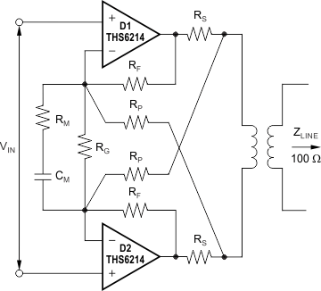 Figure 87. 0.1-dB Flatness Compensation Circuit
8.2.2.2.2 Total Driver Power for xDSL Applications
The total internal power dissipation for the THS6214 in an xDSL line driver application is the sum of the quiescent power and the output stage power. The THS6214 holds a relatively constant quiescent current versus supply voltage—giving a power contribution that is simply the quiescent current times the supply voltage used (the supply voltage is greater than the solution given in Equation 15). The total output stage power can be computed with reference to Figure 88.
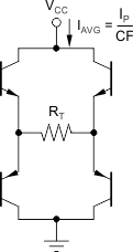 Figure 88. Output Stage Power Model
The two output stages used to drive the load of Figure 85 are shown as an H-Bridge in Figure 88. The average current drawn from the supply into this H-Bridge and load is the peak current in the load given by Equation 13 divided by the crest factor (CF) for the xDSL modulation. This total power from the supply is then reduced by the power in RT, leaving the power dissipated internal to the drivers in the four output stage transistors. That power is simply the target line power used in Equation 8 plus the power lost in the matching elements (RM). In the following examples, a perfect match is targeted giving the same power in the matching elements as in the load. The output stage power is then set by Equation 17.

The total amplifier power is then given by Equation 18:

For the ADSL CO driver design of Figure 84, the peak current is 159 mA for a signal that requires a crest factor of 5.6 with a target line power of 20.5 dBm into a 100-Ω load (115 mW).
With a typical quiescent current of 21 mA and a nominal supply voltage of ±12 V, the total internal power dissipation for the solution of Figure 84 is given by Equation 19:
