SBOS746A June 2016 – February 2021 THS6302
PRODUCTION DATA
- 1 Features
- 2 Applications
- 3 Description
- 4 Revision History
- 5 Pin Configuration and Functions
- 6 Specifications
- 7 Detailed Description
- 8 Application and Implementation
- 9 Power Supply Recommendations
- 10Layout
- 11Device and Documentation Support
- 12Mechanical, Packaging, and Orderable Information
Package Options
Mechanical Data (Package|Pins)
- RHF|28
Thermal pad, mechanical data (Package|Pins)
- RHF|28
Orderable Information
5 Pin Configuration and Functions
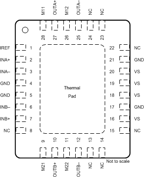
 Figure 5-1 RHF Package28-Pin VQFNTop View
Table 5-1 Pin Functions
| PIN | I/O | DESCRIPTION | |
|---|---|---|---|
| NAME | NO. | ||
| IREF | 1 | — | Bias current reference pin |
| INA+ | 2 | I | Positive input for channel A |
| INA– | 3 | I | Negative input for channel A |
| INB+ | 7 | I | Positive input for channel B |
| INB– | 6 | I | Negative input for channel B |
| OUTA+ | 27 | O | Positive output for channel A |
| OUTA– | 25 | O | Negative output for channel A |
| OUTB+ | 10 | O | Positive output for channel B |
| OUTB– | 12 | O | Negative output for channel B |
| M11 | 28 | I | Most significant bit (MSB) of channel A |
| M12 | 26 | I | Least significant bit (LSB) of channel A |
| M21 | 9 | I | MSB of channel B |
| M22 | 11 | I | LSB of channel B |
| VS | 16, 18, 19, 20 | — | Positive supply voltage connection |
| GND | 4, 5, 17, 21 | — | Ground |
| NC | 8, 13, 14, 15, 22, 23, 24 | — | Not connected |
| Thermal pad | — | Device thermal pad, connected to ground | |