SLLSEY4A July   2017  – November 2018 THVD1500

PRODUCTION DATA.  

  1. Features
  2. Applications
  3. Description
    1.     Device Images
      1.      Simplified Schematic
  4. Revision History
  5. Pin Configuration and Functions
    1.     Pin Functions
  6. Specifications
    1. 6.1 Absolute Maximum Ratings
    2. 6.2 ESD Ratings
    3. 6.3 Recommended Operating Conditions
    4. 6.4 Thermal Information
    5. 6.5 Power Dissipation
    6. 6.6 Electrical Characteristics
    7. 6.7 Switching Characteristics
    8. 6.8 Typical Characteristics
  7. Parameter Measurement Information
  8. Detailed Description
    1. 8.1 Overview
    2. 8.2 Functional Block Diagrams
    3. 8.3 Feature Description
    4. 8.4 Device Functional Modes
  9. Application and Implementation
    1. 9.1 Application Information
    2. 9.2 Typical Application
      1. 9.2.1 Design Requirements
        1. 9.2.1.1 Data Rate and Bus Length
        2. 9.2.1.2 Stub Length
        3. 9.2.1.3 Bus Loading
        4. 9.2.1.4 Receiver Failsafe
        5. 9.2.1.5 Transient Protection
      2. 9.2.2 Detailed Design Procedure
      3. 9.2.3 Application Curves
  10. 10Power Supply Recommendations
  11. 11Layout
    1. 11.1 Layout Guidelines
    2. 11.2 Layout Example
  12. 12Device and Documentation Support
    1. 12.1 Device Support
    2. 12.2 Third-Party Products Disclaimer
    3. 12.3 Receiving Notification of Documentation Updates
    4. 12.4 Community Resources
    5. 12.5 Trademarks
    6. 12.6 Electrostatic Discharge Caution
    7. 12.7 Glossary
  13. 13Mechanical, Packaging, and Orderable Information

Package Options

Refer to the PDF data sheet for device specific package drawings

Mechanical Data (Package|Pins)
  • D|8
Thermal pad, mechanical data (Package|Pins)
Orderable Information

Typical Characteristics

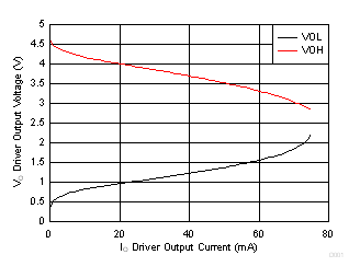
THVD1500 D001_SLLSEY4.gif
VCC = 5 V DE = VCC
Figure 1. Driver Output voltage vs Driver Output Current
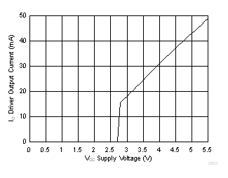
THVD1500 D003_SLLSEY4.gif
RL = 54 Ω DE = VCC D = VCC
TA = 25°C
Figure 3. Driver Output Current vs Supply Voltage
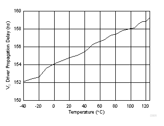
THVD1500 D005_SLLSEY4.gif
Figure 5. Driver Propagation Delay vs Temperature
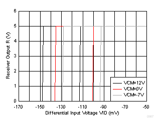
THVD1500 D007_SLLSEY4.gif
Figure 7. Receiver Output vs Input
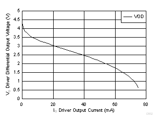
THVD1500 D002_SLLSEY4.gif
VCC = 5 V DE = VCC D = 0 V
Figure 2. Driver Differential Output voltage vs Driver Output Current
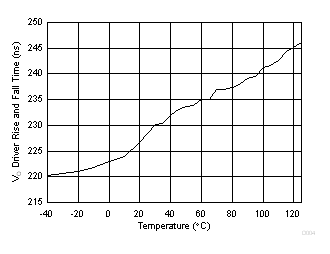
THVD1500 D004_SLLSEY4.gif
Figure 4. Driver Rise or Fall Time vs Temperature
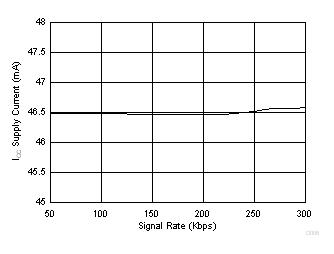
THVD1500 D006_SLLSEY4.gif
RL = 54 Ω
Figure 6. Supply Current vs Signal Rate