SLLSEV1C September   2017  – December 2018 THVD1510 , THVD1512 , THVD1550 , THVD1551 , THVD1552

PRODUCTION DATA.  

  1. Features
  2. Applications
  3. Description
    1.     Device Images
      1.      THVD1510 and THVD1550 Simplified Schematic
      2.      THVD1551 Simplified Schematic
      3.      THVD1512 and THVD1552 Simplified Schematic
  4. Revision History
  5. Device Comparison Table
  6. Pin Configuration and Functions
    1.     Pin Functions
    2.     Pin Functions
    3.     Pin Functions
  7. Specifications
    1. 7.1 Absolute Maximum Ratings
    2. 7.2 ESD Ratings
    3. 7.3 Recommended Operating Conditions
    4. 7.4 Thermal Information
    5. 7.5 Power Dissipation
    6. 7.6 Electrical Characteristics
    7. 7.7 Switching Characteristics
    8. 7.8 Switching Characteristics
    9. 7.9 Typical Characteristics
  8. Parameter Measurement Information
  9. Detailed Description
    1. 9.1 Overview
    2. 9.2 Functional Block Diagrams
    3. 9.3 Feature Description
    4. 9.4 Device Functional Modes
      1. 9.4.1 Device Functional Modes for THVD1510 and THVD1550
      2. 9.4.2 Device Functional Modes for THVD1551
      3. 9.4.3 Device Functional Modes for THVD1512 and THVD1552
  10. 10Application and Implementation
    1. 10.1 Application Information
    2. 10.2 Typical Application
      1. 10.2.1 Design Requirements
        1. 10.2.1.1 Data Rate and Bus Length
        2. 10.2.1.2 Stub Length
        3. 10.2.1.3 Bus Loading
        4. 10.2.1.4 Receiver Failsafe
        5. 10.2.1.5 Transient Protection
      2. 10.2.2 Detailed Design Procedure
      3. 10.2.3 Application Curves
  11. 11Power Supply Recommendations
  12. 12Layout
    1. 12.1 Layout Guidelines
    2. 12.2 Layout Example
  13. 13Device and Documentation Support
    1. 13.1 Device Support
    2. 13.2 Third-Party Products Disclaimer
    3. 13.3 Related Links
    4. 13.4 Receiving Notification of Documentation Updates
    5. 13.5 Community Resources
    6. 13.6 Trademarks
    7. 13.7 Electrostatic Discharge Caution
    8. 13.8 Glossary
  14. 14Mechanical, Packaging, and Orderable Information

Package Options

Refer to the PDF data sheet for device specific package drawings

Mechanical Data (Package|Pins)
  • D|14
  • DGS|10
Thermal pad, mechanical data (Package|Pins)
Orderable Information

Detailed Design Procedure

Figure 28 and Figure 29 suggest a protection circuit against 1 kV surge (IEC 61000-4-5) transients. Table 7 shows the associated bill of materials.
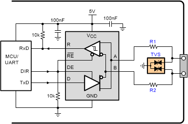
THVD1510 THVD1512 THVD1550 THVD1551 THVD1552 trans_prot_half_duplex_sllsev1.gifFigure 28. Transient Protection Against Surge Transients for Half-Duplex Devices
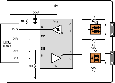
THVD1510 THVD1512 THVD1550 THVD1551 THVD1552 trans_prot_full_duplex_sllsev1.gifFigure 29. Transient Protection Against Surge Transients for Full-Duplex Devices

Table 7. Bill of Materials

DEVICE FUNCTION ORDER NUMBER MANUFACTURER
XCVR 5-V, RS-485 transceiver THVD15xx TI
R1 10-Ω, pulse-proof thick-film resistor CRCW0603010RJNEAHP Vishay
R2
TVS Bidirectional 400-W transient suppressor CDSOT23-SM712 Bourns