SLLSFD6A May   2020  – March 2021 THVD8000

PRODUCTION DATA  

  1. Features
  2. Applications
  3. Description
  4. Revision History
  5. Pin Configuration and Functions
  6. Specifications
    1. 6.1 Absolute Maximum Ratings
    2. 6.2 ESD Ratings
    3. 6.3 ESD Ratings - IEC Specifications
    4. 6.4 Recommended Operating Conditions
    5. 6.5 Thermal Information
    6. 6.6 Electrical Characteristics
    7. 6.7 Power Dissipation Characteristics
    8. 6.8 Switching Characteristics
    9. 6.9 Typical Characteristics
  7. Parameter Measurement Information
  8. Detailed Description
    1. 8.1 Overview
    2. 8.2 Functional Block Diagrams
    3. 8.3 Feature Description
      1. 8.3.1 OOK Modulation with F_SET pin
      2. 8.3.2 OOK Demodulation
      3. 8.3.3 Transmitter Timeout
      4. 8.3.4 Polarity Free Operation
      5. 8.3.5 Glitch Free Mode Change
      6. 8.3.6 Integrated IEC ESD and EFT Protection
    4. 8.4 Device Functional Modes
      1. 8.4.1 OOK Mode
      2. 8.4.2 Thermal shutdown (TSD)
  9. Application Information Disclaimer
    1. 9.1 Application information
    2. 9.2 Typical application (OOK mode)
      1. 9.2.1 Design requirements
        1. 9.2.1.1 Carrier frequency
      2. 9.2.2 Detailed design procedure
        1. 9.2.2.1 Inductor value selection
        2. 9.2.2.2 Capacitor value selection
      3. 9.2.3 Application Curves
  10. 10Power supply recommendations
  11. 11Layout
    1. 11.1 Layout guidelines
    2. 11.2 Layout Example
  12. 12Device and Documentation Support
    1. 12.1 Device Support
    2. 12.2 Receiving Notification of Documentation Updates
    3. 12.3 Support Resources
    4. 12.4 Trademarks
    5. 12.5 Electrostatic Discharge Caution
    6. 12.6 Glossary

Package Options

Mechanical Data (Package|Pins)
Thermal pad, mechanical data (Package|Pins)
Orderable Information

Capacitor value selection

Capacitor selection is easier than inductor selection, primarily because capacitance impedance is important to allow higher frequency signals through. However, the capacitor ratings for voltage must be carefully selected to meet the application requirements. Special considerations for hot plug nodes should be made to ensure that voltage transients during hot plugging do not exceed the absolute maximum values. See Section 6.1.

The number of nodes on the bus does not play into the capacitance calculation. The impedance of a capacitor is shown in Equation 4.

Equation 4. GUID-8761E445-0814-44AF-9EE4-0AF23ACA5C37-low.gif

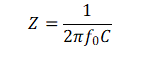
Maintaining Z ≤ 5 Ω keeps the impedance low enough at the carrier frequency to allow data to pass through. If the equation is rearranged to calculate C, the result is shown in Equation 5.

Equation 5. GUID-561A7C5D-8520-47D5-A986-13514547A1BD-low.gif

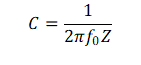
If the previous example of a 1 MHz carrier frequency is used, then a minimum capacitance value of about 32 nF. For a quick reference, refer to Figure 9-3.